- Home
- Users & Science
- Scientific Documentation
- ESRF Highlights
- ESRF Highlights 2007
- X-ray Absorption and Magnetic Scattering
- Depth-resolved study of impurity sites in low-energy ion-implanted As in Si
Depth-resolved study of impurity sites in low-energy ion-implanted As in Si
The electrical and diffusion properties of dopant atoms in silicon are of primary importance for the realisation of ultra-shallow junctions for transistors in the semiconductor industry. In arsenic-doped Si:As, important phenomena appear when the doping level reaches volumes as high as 1021 cm–3, namely: (i) the concentration of free carriers does not increase linearly with the doping level; (ii) rapid thermal annealing (RTA) enhances the concentration of active carriers, while further annealing decreases the number of electrically-active impurities to saturation levels; (iii) the As diffusion coefficient starts to increase rapidly. Furthermore, upon RTA the original implant profile is modified significantly by the transient enhanced diffusion effect, generating long tails of dopants into the substrate and their accumulation near the surface. To explain the electrical As deactivation and its enhanced diffusion one can use X-ray measurements and computer simulation techniques. The extended X-ray absorption fine structure (EXAFS) technique has been widely used since it characterises the local atomic structure around the dopant atom. The efficacity of ab initio calculations to reproduce the local structure of point defects has also been demonstrated.
In this work we combine EXAFS measurements and ab initio total energy calculations to investigate these phenomena. In particular, we investigated four crystalline Si:As samples, obtained by implanting Si (001) substrates with As+ ions at an energy of 5 keV and a fluence of 1x1015cm–2 and treated by different thermal budgets.
The EXAFS measurements were carried out at the arsenic K edge (E = 11867 eV) in glancing angle geometry, at BM08, the GILDA CRG beamline. For each sample, spectra were collected in total reflection (TR), and high angle (HA) modes. TR uses an incident beam below the critical angle for the total reflection, and the latter above, so that the As site in surface part (about 6 nm in TR mode) or in the bulk (300 nm in HA mode) of the sample are probed.
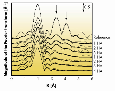
The experimental findings were supported by our theoretical study based on the density functional theory (DFT). Figure 107 shows the Fourier Transform pattern of the EXAFS spectra of the samples measured both in TR and HA. The reference used for As in a substitutional position is the spectrum of an Si (001) wafer implanted with As+ ions at an energy of 70 keV and a fluence of 3x1015 cm–2 and annealed at 1100°C in N2 for 100 s.
 |
|
Fig. 107: Fourier transform patterns of the raw EXAFS spectra (lines) compared with the best fit curves (dots). The spectra numbers identify the sample treatment: 1 corresponds to RTA at 900°C, 2 to RTA at 1050°C, 3 to spike annealing at 1050°C, 4 to the as implanted. The reference sample is described in the text. |
Arrows indicate the peaks that exhibit the more marked change when passing from HA to TR series. In our case, the peaks located in the region from 3.0 to 4.5 Å correspond to the second and third coordination shells. They are weaker in the HA spectra than those in the reference spectrum and they disappear in the TR spectra. This indicates an increase of the disorder in all the samples, which is more evident in the shallow region.
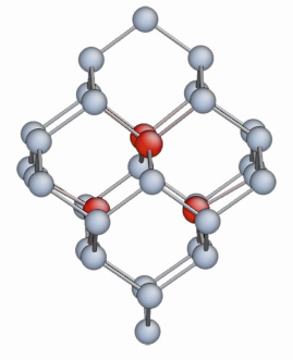
The HA data, relative to all the As content, also in the deeper part of the implant, reveal the presence of As in the Si matrix linked to a vacancy. Only by comparing the value of the distance for Si second neighbours resulting from the fit of the experimental data and those obtained by DFT calculations for various complexes V-Asn (n=1 to 4) we could identify V-As3 and V-As4 as those present in the material. Figure 108 represents a model of the V-As4 complex.
 |
|
Fig. 108: Balls and sticks representation of the V-As4 complex. |
In the TR case we found a very disordered environment with possible presence of As precipitates. This is due to the crystallisation front that, initiating from the amorphous/crystalline interface during the annealing, transports dopants towards the Si/SiO2 interface (snowplough effect) creating in this zone an increased concentration of As impurities and defects.
In this work we have carried out a depth-selective EXAFS investigation in grazing incidence geometry on arsenic doped silicon samples. Evidence of different environments of the impurity along the concentration profile has been found and the experimental findings have been compared with an ab initio study. In summary, As occupies predominantly substitutional positions and it is linked to vacancies forming As3V and/or As4V complexes. Conversely, near the surface, the local structure appears to be extremely disordered, plausibly as a consequence of the As accumulation at the surface due to the thermal annealing treatment.
References
[1] A. Lietoila, J.F. Gibbons and T. W. Sigmon, Appl. Phys. Lett. 36 (9), 765 (1980).
[2] M. Ramamoorthy and S. T. Pantelides, Phys. Rev. Lett. 76 (25), 4753 (1996).
[3] A. Satta, E. Albertazzi, G. Lulli and L. Colombo, Phys. Rev. B 72 (23), 235206 (2005).
Principal publication and authors
F. d’Acapito (a), S. Milita (b), A. Satta (c), L. Colombo (c,d) , J. Appl. Phys. 102, 043524 (2007).
(a) CNR-INFM-OGG, GILDA CRG Grenoble (France)
(b) CNR-IMM, Bologna (Italy)
(c) CNR-INFM SLACS Cagliari (Italy)
(d) Dept. of Physics University of Cagliari (Italy)


