- Home
- Users & Science
- Scientific Documentation
- ESRF Highlights
- ESRF Highlights 2009
- Structure of materials
- Squeezing single nanostructures
Squeezing single nanostructures
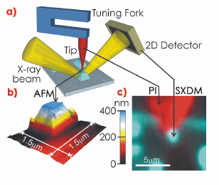
The spatial confinement of low-dimensional materials can influence their physical properties. The plastic regime has been investigated by nanoindentation, compression and tensile tests, whereas the elastic properties of individual nanoscale objects such as single nanowires were studied and contradictory results reported on the size dependence of Young’s modulus. In order to study the elastic properties of individual nanostructures we combined micro X-ray diffraction (µXRD) and an in situ atomic force microscope (AFM, Small Infinity) which allows both topographical imaging of the sample surface and selection of a specific nanoobject. The electrochemically blunted AFM tungsten tip can be used to deform an object by applying a well-defined force. The experimental setup is presented in Figure 34a. During the application of pressure, µXRD images are simultaneously recorded giving direct access to the lattice deformation in the object. For alignment of the sample, the AFM tip, and the microfocussed X-ray beam, we employ scanning X-ray diffraction mapping (SXDM) and photocurrent imaging (PI). The focussed X-ray beam is scanned across the sample and the X-ray signal of the nanoobjects is recorded resulting in a positional 2D map of the structures. When the X-ray beam hits the AFM tip, photoelectrons are emitted inducing a photocurrent which is simultaneously recorded with the SXDM, facilitating the alignment.
In the present study, we investigated the elastic properties of individual SiGe islands, at beamline ID01. Figures 34b and 34c present an AFM image of a SiGe island and a superposition of a scanning X-ray diffraction map and a PI image, respectively. Figure 34c demonstrates the excellent alignment employing these two imaging techniques simultaneously.
 |
|
Fig. 34: a) Schematic of the experimental setup. b) Atomic force micrograph of a SiGe island. c) Superposition of simultaneous SXDM (blue) and PI (red) images. |
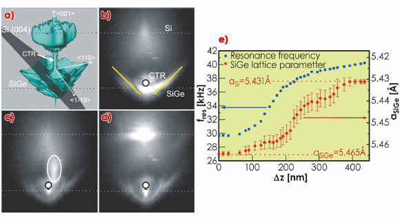
Figure 35a shows the calculated three-dimensional reciprocal space map (3D-RSM) of a SiGe island grown on a Si(001) substrate. In the experiment, a two-dimensional detector is used, cutting through reciprocal space and thus recording only a 2D-RSM. The corresponding detector plane is represented by the semitransparent plane in Figure 35a. The related XRD pattern is displayed in Figure 35b showing the substrate Bragg peak (Si(004)), the crystal truncation rod of the substrate, and the signal of the SiGe island including the truncation rods originating from the island’s {111} side facets. Figures 35c and 35d display the XRD patterns for the SiGe island under different pressures. For the highest pressure, the SiGe island intensity maximum is superimposed onto the Si substrate peak. Thus, the change in lattice parameter of the island can be followed in situ as a function of the applied pressure.
 |
|
Fig. 35: a) Calculated 3D-RSM of an SiGe island in the vicinity of the Si(004) Bragg peak. The semitransparent plane depicts the interception of the reciprocal space by the detector plane for the images (b-d). b) 2D µXRD pattern of a non-compressed island. The flares (yellow lines) originate from the truncation rods of the island’s {111} side facets. c) and d) the same X-ray maps for different pressures. e) Variation of both the SiGe island lattice parameter and the tuning fork resonance frequency as a function of the piezo travel |
To quantify these results, the lattice parameter a of the SiGe island under investigation as a function of the piezo travel is presented in Figure 35e. In addition, the resonance frequency f (which is related to the applied force) of the AFM force sensor – a quartz tuning fork – is displayed shifting to larger values with increasing force applied. The two parameters, a and f, follow each other revealing a direct correlation between them. The shift of the resonance frequency originates from the stiffness of the contact area between the AFM tip and the island. This contact stiffness S can be derived by employing the Hertzian contact model. The effective Young’s modulus of the system consisting of the SiGe island and the tungsten tip, was determined from the data S and a as 108 GPa. This is in excellent agreement with the bulk value of 105 GPa. Moreover, the pressure needed to compress the island lattice to the value of pure Si is in very good accordance with finite-element method calculations using bulk properties. Thus, no size effects of the elastic properties were found as expected for islands of this size (1 µm base length). The excellent agreement of experiment and theory demonstrates the very good performance of the in situ combination of AFM and µXRD and opens the door to in situ elasticity studies of nanostructures.
The in situ AFM tuning fork allows the determination of frequency shifts ranging from 0.1 to 104 Hz and hence cover five orders of magnitude. Owing to the direct correlation between elastic modulus and frequency shift, a broad class of materials can be investigated ranging from soft to hard matter.
Principal publication and authors
T. Scheler (a), M. Rodrigues (a), T.W. Cornelius (a), C. Mocuta (a), A. Malachias (a), R. Magalhães-Paniago (a), F. Comin (a), J. Chevrier (a,b) and T.H. Metzger (a), Appl. Phys. Lett. 94, 023109 (2009);
M.S. Rodrigues (a), T.W. Cornelius (a), T. Scheler (a), C. Mocuta (a), A. Malachias (a), R. Magalhães-Paniago (a), F. Comin (a), T.H. Metzger (a) and J. Chevrier (a,b), J. Appl. Phys. 106, 103525 (2009).
(a) ESRF
(b) Institut Néel, CNRS-UJF, Grenoble (France)


