- Home
- Users & Science
- Scientific Documentation
- ESRF Highlights
- ESRF Highlights 2011
- Enabling technologies
- HIZPAD, a European collaboration for the development of pixel detectors dedicated to high X-rays energies
HIZPAD, a European collaboration for the development of pixel detectors dedicated to high X-rays energies
HIZPAD (high-Z pixel array detectors) is a Joint Research Activity of the ELISA European project that started in March 2009 and was completed in August 2011. HIZPAD focused on the evaluation of existing high-Z pixel sensor technologies for application to X-ray pixel detectors used at synchrotron radiation and free electron laser sources. This initiative emerged from the need to improve the detection efficiency of X-ray pixel detectors in the 20-100 keV energy range, limited by the poor absortion of the thin (300-500 µm) silicon sensors currently in use. HIZPAD was coordinated by the ESRF and gathered the major European synchrotron radiation sources as well as leading European institutes and companies in the field of pixelated semiconductor detectors.
The work programme started by a survey that included: the high-Z pixel detector needs of synchrotron radiation and free electron laser sources (carried out by SOLEIL); high-Z materials performance and sensors suppliers (Freiburger Materialforschungsinstitut (FMF), and the University of Surrey) and high-Z pixel sensor hybridisation technologies and suppliers (STFC). The survey clearly showed that CdTe and possibly CZT were the only viable options for the high-Z pixel sensor material given the time frame of our project. It also allowed us to identify the most advanced industrial providers for sensor materials and processing.
After assessment of the electrical performance of the sensor materials by the University of Surrey and by FMF, a collection of CdTe pixel sensors with pixel pitches from 55 to 172 µm and detection areas from 2 to 14 cm2 were produced and bump-bonded by X-ray Imaging Europe (XIE) to TIMEPIX [1], XPAD, and PILATUS photon-counting readout chips. CdTe linear microstrips connected to a MYTHEN readout system were also produced by PSI. A few CZT sensors were also made for later evaluation.
The CdTe assemblies were then integrated into test detectors and an extensive characterisation was carried out at the ESRF [2], DESY, SOLEIL, DLS and PSI, from which we can outline the following results:
Although made of the highest grade material available, the CdTe sensors all exhibited varying amounts of insensitive regions of a few tens of pixels wide, the origin of which is still to be identified. Accepting those defects, a flatfield correction generally allowed quite a uniform image to be obtained. The sensor coupling to the readout chips remains a delicate operation and some failures were experienced.
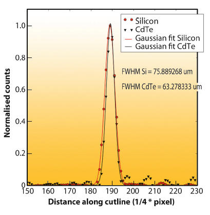
We measured a spatial resolution of 65 µm (PSF FWHM) on 55 µm pixel pitch CdTe assemblies in the 22-90 keV energy domain. At 22 keV, the spatial resolution is even found slightly better than with silicon pixel devices of same pixel size (Figure 149).
 |
|
Fig. 149: Line-spread function of CdTe and of Si pixel sensors of same pitch (55 µm) at 22 keV, normalised to the same intensity. |
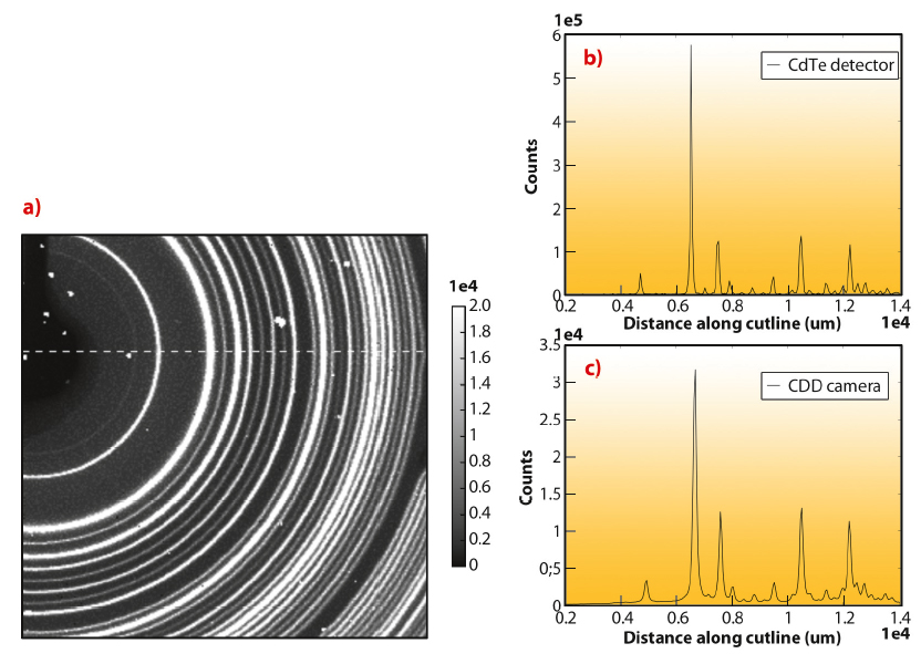
In a powder diffraction experiment carried out at ID11, a materials science beamline, we compared a CdTe pixel test detector with a CCD-based X-ray detector of similar pixel size. At 50 keV, the CdTe pixel device produced a signal that was 10-times higher than that of the CCD-based detector, and in addition it had better spatial resolution and efficient filtering of low energy background noise (Figure 150).
In conclusion, the HIZPAD collaboration demonstrated the feasibility as well as the high interest of high-Z pixel devices for synchrotron radiation and free electron laser applications, particularly those for materials science. A key result is the dramatic increase in detection efficiency without loss in spatial resolution. Developments initiated in HIZPAD will be continued with a focus on the reduction of sensor defects as well as on the increase of detection areas.
Authors
C. Ponchut and M.Ruat
ESRF
References
[1] X. Llopart, R. Ballabriga, M. Campbell, L. Tlustsos and W. Wong, Nucl. Instr. and Meth. A 581, 485 (2007); and erratum Nucl. Instr. Meth. A 585, 106 (2008).
[2] M. Ruat and C. Ponchut, Proceedings of the IEEE conference RTSD workshop, Valencia, Submitted to Trans. Nucl. Sci. (2011).
Acknowledgment
The authors are grateful to J. Wright and G. Vaughan from ID11, V. Honkimaki, T. Buslaps and C. Chabert from ID15, E. Ziegler and T. Lafford from BM05, C. Nemoz, T. Brochart and A. Bravin from ID17, for giving access to beamtime, and also for their support and involvement during tests campaigns. The research leading to these results has received funding from the European Community’s Seventh Framework Programme (FP7/2007-2013) under grant agreement nº 226716. The MEDIPIX2 and TIMEPIX readout chips are developed by CERN and the Medipix2 collaboration.


