- Home
- Users & Science
- Scientific Documentation
- ESRF Highlights
- ESRF Highlights 2012
- X-ray imaging
- Imaging the geometrical carrier confinement within a single core-multishell nanowire
Imaging the geometrical carrier confinement within a single core-multishell nanowire
Nanostructures made from organic and inorganic materials have been extensively characterised using luminescence-related techniques with spectral and temporal resolution. However, obtaining information on individual nanostructures rather than ensembles is a challenge for photoluminescence techniques. X-ray excited optical luminescence (XEOL) is a synchrotron soft X-ray technique that typically suffers from poor spatial resolution and long carrier diffusion length [1]. But recently, this technique has become particularly attractive for imaging certain optical phenomena in nanotechnology by making use of quantum confinement to limit the carrier dynamics. Here, a study of geometrical confinement effects in core-multishell nanowires shows that the hard X-ray approach at the nanoscale can provide new information. This imaging method combines XEOL with simultaneous X-ray fluorescence (XRF) spectroscopy using a nanometre-sized hard X-ray beam.
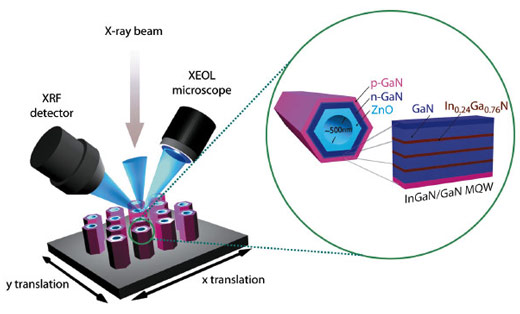
Figure 67 shows a schematic of the experimental setup at ID22NI [2]. Using a pair of Kirkpatrick-Baez Si mirrors, the X-ray nanobeam (60 x 60 nm2 with 1012 ph/s at 29.6 keV) impinges on the sample, which emits luminescence and XRF photons. XEOL and XRF spectra are recorded with a far-field optics system and a silicon drift detector, respectively, for each raster position of the sample. As a proof of concept, we have applied this technique to p-GaN/In1-xGaxN/n-GaN/ZnO nanowires grown by metal-organic vapour phase epitaxy. Recent calculations indicate that the modulation of the radial elemental composition within a nanoscale hexagonal geometry introduces new complexities that create novel confinement effects [3]. Figure 67 also displays a magnified cross-sectional view of the nanowires, highlighting the GaN/InGaN multiquantum-well (MQW) structure.
 |
|
Fig. 67: Schematic of the hard X-ray nanoprobe experimental setup and magnified cross-sectional view of a GaN/In1-xGaxN/GaN/ZnO nanowire heterostructure, highlighting the GaN/InGaN multiquantum-well. |
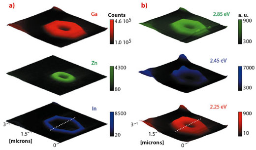
Figure 68 shows results obtained by scanning the nanowire along the radial direction for nano-XRF and nano-XEOL. The measurements identify the precise spatial location of the nanowire and reveal several points: The three-dimensional representation of the XRF data shows that the major elements exhibit high contrast, indicative of uniform core-multishell encapsulation in the radial chemical composition consistent with the targeted heterostructure. Within the sensitivity of our experimental setup, the sharp elemental images suggest that no significant interdiffusion took place across individual shells. The corresponding XEOL maps reveal three principal emission bands: a shoulder at 2.25 eV attributed to the common yellow band from point defects in GaN (probably Ga vacancies), a dominant green line at 2.45 eV attributed to the transitions from the In0.24Ga0.76N/GaN MQWs, and a weak blue peak at 2.85 eV attributed to the band-to-acceptor emission of the outmost Mg-doped GaN layer. The 3-D projection of the emissions located at 2.25 and 2.85 eV exhibits a uniform distribution of gallium vacancies and impurities, in good agreement with the XRF results. In contrast, the 3-D illustration of the band emitted at 2.45 eV indicates that the InGaN-related emissions radiate mainly from the six corners of the hexagon. The latter characteristic strongly suggests the existence of additional carrier confinement effects.
Although inhomogeneous distribution of indium and/or small well thickness fluctuations could be the source of the higher intensity of InGaN-related emission at the hexagon corners, the image corresponding to the linewidth (not shown here) actually illustrates a reduction of peak broadening with a small but clear blue energy shift. These findings result from the enhanced carrier confinement within the MQWs merging at the corners, and have been confirmed through a theoretical investigation. A higher confinement of the wave function at the hexagon corners is observed in remarkable consistence with the XEOL results. There is a finite charge separation over the hexagon, which results in an overall greater overlap between the wave functions of electrons and holes at the corners.
In summary, the observation of the carrier confinement effects under hexagonal cross-section in single core-multishell nanowires presented here gives a glimpse of the new research directions such a hyperspectral imaging method can provide. It represents a step towards the validation of theories of quantum confinement for nanodevices, and also the realisation of nanostructures with spectroscopic properties that could prove advantageous not only in light-emitting diodes but also in biological labelling experiments in life science. Its great potential becomes more valuable when time resolving power is added, as well as when this technique is used in conjunction with other methods, such as X-ray absorption spectroscopy and X-ray diffraction characterisation.
Principal publication and authors
G. Martínez-Criado, A. Homs, B. Alén, J.A. Sans, J. Segura-Ruiz, A. Molina-Sánchez, J. Susini, J. Yoo and G.-C. Yi, Nano Lett. 12, 5829-5834 (2012).
ESRF
References
[1] A. Rogalev and J. Goulon, X-ray Excited Optical Luminescence Spectroscopies, Chemical Applications of Synchrotron Radiation Part II, World Scientific: Singapore (2002).
[2] G. Martinez-Criado et al., J. Synchrotron Rad. 19, 10 (2012).
[3] B.M. Wong et al., Nano Lett. 11, 3074 (2011).


