- Home
- Users & Science
- Scientific Documentation
- ESRF Highlights
- ESRF Highlights 2012
- Structure of materials
- Three-dimensional microscopy of extended crystals through X-ray Bragg ptychography
Three-dimensional microscopy of extended crystals through X-ray Bragg ptychography
Understanding the growth mechanisms of bio-mineralised sea-shells or improving the performances of optical, mechanical or electronic devices requires a detailed knowledge of crystalline properties at the nanoscale. This motivates the development of powerful characterisation techniques for strain determination. Today, X-ray lens-less microscopy, exploiting the coherence properties of third-generation synchrotron sources, is gaining a larger place among the classical imaging techniques. This technique is quantitative, non-invasive, and provides a resolving power meeting the requirements of nanoscience. In this approach, the lenses are advantageously replaced by inversion algorithms: all the information about the inside structure of the sample can be reconstructed from the coherently scattered intensity, without specific sample preparation. By means of this imaging approach, the details about shape and chemical composition of crystalline nanostructures are obtained. The high sensitivity to the displacement field in the crystal is provided by the Bragg geometry, which allows additional strain information [1].
One main limit is defined by the size of the field of view, which is of the order of a few micrometres. The use of ptychography [2] has been proposed to extend the field of view without degrading the image resolution. Ptychography (from the Greek for “fold”) is a technique originally developed for electron microscopes and recently expanded to X-rays in the forward scattering direction to image the morphology of extended samples [2]. It is based on the redundancy of the information taken from partially-overlapping illumination areas on an extended sample. A set of far-field coherent intensity patterns is recorded while the sample is moved through the finite-sized beam spot. The redundancy, resulting from the overlapping condition, is the key of the iterative process convergence and, consequently, of a successful reconstruction of the sample.
The extension of this method to the Bragg case is a development successfully exploited in this work. In this case, the full 3D Bragg diffraction pattern is recorded at each position of the beam on the sample. The whole set of data is fed into a Bragg-adapted algorithm which allows the retrieval of the sample image.
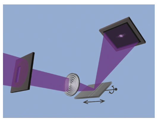
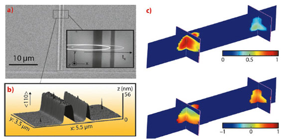
Figure 107 shows the schematic layout of the experimental setup. The coherent finite-sized beam spot needed for the ptychography scan is obtained by a Fresnel zone plate (FZP) illuminated in an area that matches the beam transverse coherence lengths. As the FZP central part is occluded by a beam stop to avoid direct beam contribution, the aperture is shifted laterally. The sample, patterned from a silicon-on-insulator wafer is composed of two Si <110> lines of about 40 nm height and of 520 and 260 nm width, respectively (Figure 108). The separation between the lines results in an edge-to-edge distance of 1.7 μm. The line length is about 30 μm, much larger than the beam footprint. The areas delimited by the white ellipses correspond to the first positions of the beam during the scan.
The 3D intensity frames recorded in each point of the ptychographical scan are fed into the inversion algorithms. Together with the morphology of the sample, the displacement field is also imaged in radian units.
Bragg ptychography makes the three-dimensional imaging of crystals by X-ray microscopy possible by overcoming the size constraint for samples. That is in addition to providing crystal-specific information such as strain fields or the presence of defects in the crystalline structure. This first demonstration paves the way for the exploration of a wide range of crystalline materials, belonging to such diverse fields as life sciences and microelectronics.
Principal publication and authors
P. Godard (a), G. Carbone (b), M. Allain (a), F. Mastropietro (b,c), G. Chen (d), L. Capello (e), A. Diaz (b), T.H. Metzger (b), J. Stangl (d) and V. Chamard (a), Nature Communications 2, 568 (2011).
(a) Institut Fresnel, Aix-Marseille University, CNRS, Marseille (France)
(b) ESRF
(c) CEA/Grenoble SP2M/Nano-structures et Rayonnement Synchrotron, Grenoble (France)
(d) Institute of Semiconductor and Solid State Physics, Johannes Kepler Universität, Linz (Austria)
(e) Soitec S.A., Parc Technologique des Fontaines, Bernin (France)
References
[1] M.C. Newton, S.J. Leake, R. Harder and I.K. Robinson, Nature Mater. 9, 120 (2010).
[2] M. Dierolf, A. Menzel, P. Thibault, P. Schneider, C.M. Kewish, R. Wepf, O. Bunk and F. Pfeiffer, Nature 467, 436 (2010).


