- Home
- Industry
- Industry news
- The ESRF characterises...
The ESRF characterises 3D integration systems in microelectronics
30-06-2018
The ESRF is helping the microelectronics industry to characterise 3D integration systems, which aims to make devices smaller. A new publication by scientists from the CEA, ST Microelectronics and the ESRF lays it all bare.
Share
In the microelectronics industry, one possible way to make the devices smaller is to stack the wafers in the vertical direction instead of setting them next to one another. This newly created method is called 3D integration. With such a geometry, new connections have been designed in order to transmit information between the different parts of the device: they can be Through Silicon Vias (TSV), Copper Pads, or Copper Pillars (CuP).
During the assembly process, voids and other defects ranging from several nanometres to several micrometres in size can appear in the devices, changing their electrical and mechanical behaviour. Being able to characterise these materials is the key to the success of 3D integration. It is a challenging task, however, as these are three-dimensional structures, often situated in the centre of a millimetre-thick stack and not easily accessible.
A team of researchers from the CEA, ST Microelectronics and the ESRF tried different techniques to characterise in 3D copper pillars used in 3D integration. They used both destructive and non-destructive techniques. “Each of them had its own assets and drawbacks”, explains Alexandra Fraczkiewicz, PhD student at CEA and first author of the publication.
Computed tomography techniques offer good information about the voids present in the pillars and, in the case of synchrotron radiation, also about the intermetallic shapes. The contrast in synchrotron tomographies makes it easy to segment the voids inside the final volume.
“We noticed that performing successive synchrotron tomography analysis at the ESRF produces a large amount of high resolution 3D information, with a high sample throughput.”, says Pierre Bleuet, scientist at the CEA. “Our research in this case is on copper pillars, but we believe the characterisation can be extended to similar materials and dimensions in 3D integration systems or in microelectronics in general”, he adds.
 |
|
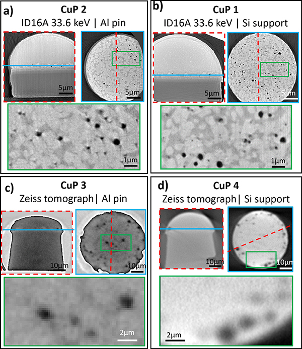
The influence of the sample geometry on the reconstructed volumes. Figures (a) and (b) show results obtained from tomographies on ID16A, with copper pillars respectively isolated on an aluminum pin (CuP 2) and placed on a silicon support (CuP 1). Figure (c) and (d) show results from the lab tomograph, with similar sample geometries (resp. CuP 3 and CuP 4). Every figure contains an XZ view of the pillar (frame indicated by dashed red line), an XY view of the interface containing voids and intermetallic alloys (frame indicated by solid blue line), and a zoom-in view of the latter (frame indicated by solid green line). |
The next step for the team is to investigate how laminography combined with ptychography can optimise even more the 3D characterisation. They believe that the combination of these two methods could provide with a large field of view, high resolution reconstructions.
This work has been possible thanks to the support of the IRT Nanoelec, a PPP (Public Private Partnership) financed by the French Government and thanks to the fact that the ESRF granted a 3-year long, innovation-lead project for this action. “It is extremely important to have development activities with a long-term perspective to create equipment adapted to industrial use, capable of tackling cutting edge technological matters and unmet needs from industry”, says Ennio Capria, Deputy Head of Business Development at the ESRF.
Reference:


