- Home
- Users & Science
- Find a beamline
- X-ray nanoprobe
- ID01 - Nano/Micro diffraction imaging
- Science on ID01
- Nanoscale mapping of SiGe quantum-electronic heterostructures
Nanoscale mapping of SiGe quantum-electronic heterostructures
Nanoscale mapping of SiGe quantum-electronic heterostructures
To observe the structure and in particular structural defects of a buried Si quantum well. It was particularly important to understand the shape and distortion of the silicon layer at length scales similar to the size of the confined electronic wavefunction, and to learn how the structure affects the splitting of the degeneracy of the valleys of the silicon bandstructure.
Background
Devices that exploit individual quantum states of electrons promise to add a new dimension to the capabilities of microelectronics. One promising route to forming these quantum structures on silicon is to create coupled quantum dots in which electrons are trapped in a thin silicon layer within a stack of layers of an alloy of silicon and germanium. As in conventional electronic devices, the properties of quantum mechanical components based on these silicon two-dimensional electron gases depend very strongly on their structure, and the changes in the structure induced by the formation of the devices. The role of specific structural defects, including atomic steps and other local sources of distortion, has been predicted theoretically and observed by electrical measurements, but has been difficult to probe in structural studies.
Synchrotron techniques
Nanodiffraction studies were carried out at beamline ID01 using a tightly focused X-ray beam. Si quantum wells in a Si/SiGe heterostructure were characterised without destructive sample preparation.
Results
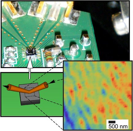
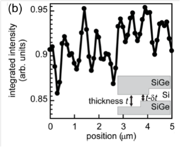
Experiments (see Figure) probed the integrated quantum dot structures and allowed the structural influence of the epitaxial growth and subsequent lithographic processing of the quantum well to be determined. The orientation, thickness, and other critical structural parameters could be extracted from these nanodiffraction experiments. In particular, the intensity of the 004 reflection of the Si quantum well (inset in the Figure) exhibits variations at the 100 nm length scale. Such intensity variations are consistent with variations of the quantum well thickness. The observed 5-10% variation corresponds to local thickness variations of approximately a single 5 Å Si unit cell. Such thickness variations can be attributed to the de-correlation of steps during epitaxial growth. Strains arising from tilts of the lattice modify the bandstructure by inducing shifts in energy levels that are comparable to the electron temperature in quantum devices.


Figure: X-ray nanodiffraction map showing the waviness in a 10 nm-thick buried Si quantum well. Structural effects at the 100-nm length scale are apparent in the total intensity of the 004 X-ray reflection of the quantum well, arising thickness variations of the order of one Si unit cell.
How did the synchrotron experiment help?
The synchrotron experiments permitted non-destructive analysis of the quantum well device integrated on a circuit board. Experiments made it possible to visualise the distortions always believed to be present in such Si/SiGe heterostructures. The knowledge gained will help to improve the fabrication processes and so to make better devices in future.
Further information
Nanoscale Distortions of Si Quantum Wells in Si/SiGe Quantum-Electronic Heterostructures
P.G. Evans, D.E. Savage, J.R. Prance, C.B. Simmons, M.G. Lagally, S.N. Coppersmith, M.A. Eriksson, T.U. Schülli, Adv. Mater. (2012)
[PGE1]ARO is the US Army Research Office. LPS refers to the quantum computing group at the University of Maryland’s Laboratory for Physical Sciences.


