- Home
- Users & Science
- Scientific Documentation
- ESRF Highlights
- ESRF Highlights 2013
- Enabling technologies
- Correlation between the lattice distortion induced by the aluminium back contact and the photovoltaic efficiency in silicon solar cells
Correlation between the lattice distortion induced by the aluminium back contact and the photovoltaic efficiency in silicon solar cells
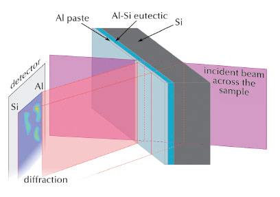
For high efficiency in silicon solar cells, the aluminium back contact is required to have low carrier recombination velocities and low series resistances. The aluminium paste for the back contact is typically screen-printed, followed by annealing and cooling, which creates eutectic and doped layers at the back surface of the silicon. Even though this technique is now used in industrial silicon solar cell manufacture, the various aluminium pastes available on the market give different photovoltaic (PV) performances. To explore this issue, the distortion and strain of the Si in contact with the Al back layer have been characterised by coupling X-ray section topography (Figure 143) at BM05 and X-ray nanodiffraction measurements at ID01. Rocking curve imaging section topography (RCIST) software was developed in order to analyse the ensemble of rocking curves and generate maps of the integrated intensity, the full width at half maximum and the peak position.
 |
|
Fig. 143: Diagram of diffraction section topography for a solar cell with Al back plane. |
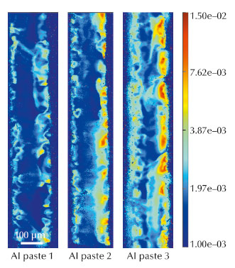
The results obtained at both BM05 and ID01 strongly suggest a correlation between the lattice distortion of the Si in contact with the eutectic and Al layers, and the photovoltaic efficiency. This distortion varies depending on the Al paste used, giving “good” and “less good” PV performance (Figure 144). The eutectic layer in the Al back contact is directly associated with the distortion and strain of the Si back surface region. The higher PV efficiency of the “good” paste appears to be related to the better homogeneity of the eutectic layer, associated with smaller distortion and strain of the Si back surface. This is directly linked to the amount of Al, Al grain size, and the precise composition of Al and other components in the different pastes. For the manufacturing process, choosing a good Al paste is therefore crucial for producing good solar cell products.
 |
|
Fig. 144: Si 220 FWHM maps (in degree) from section topography rocking curve imaging of solar cells based on mono-like Si, with Al back-planes made from the three different Al pastes. The face with the Al back plane is on the right of the virtual section image and the front side is on the left. There is clearly more distortion induced on the side with the Al back plane. Even though the mono-like Si contains many lattice defects formed during the growth, the different Al pastes clearly produce different effects - the Si 220 FWHM values vary significantly. Al paste 1 (“good” photovoltaic efficiency) causes less distortion of the Si wafer, with FWHM values as low as 2 x 10⁻³ degrees, while Al paste 3 (“less good”) induces misorientations up to 8 x 10⁻³ degrees. |
The results clearly demonstrate that synchrotron methodologies are valuable techniques for studying, not only the structure and crystalline perfection of Si, but also features associated with electrical efficiency.
Authors
T.-N. Tran Thi (a), S. Dubois (b), J. Baruchel (a), N. Enjalbert (b), M. Tsoutsouva (a), T. Schülli (a) and T. Lafford (a).
(a) ESRF
(b) CEA-INES, Savoie Technolac, Bourget du Lac (France)


