- Home
- Users & Science
- Scientific Documentation
- ESRF Highlights
- ESRF Highlights 2014
- X-ray Imaging
- Tuning the oxygen doping level in the Bi-2212 superconductor by X-ray nano-beam irradiation
Tuning the oxygen doping level in the Bi-2212 superconductor by X-ray nano-beam irradiation
The search for higher speed and lower power consumption has driven the semiconductor industry to produce increasingly smaller integrated circuits. This trend has stimulated deep innovation in the lithographic techniques based on the use of short wavelength radiation. Nevertheless, so far, hard X-rays-based lithography with λ ≈ 0.1 nm has been hampered by problems in the fabrication of suitable masks with both sufficiently high contrast in their absorbing power and small enough features. Another appealing possibility is represented by direct-writing techniques allowing the modification of substrate properties without any photoresist. Focused-electron-beam- and focused-ion-beam-induced deposition and etching, along with the scanning-probe lithography, are the most frequently used techniques, and all enabling nanometric spatial resolution [1]. A few examples of X-ray direct-writing-lithography have been reported recently, but in all cases patterning was limited to organic or organometallic materials. Since these processes are essentially based on molecular photodissociation, the limitation to this kind of materials seemed to be intrinsic to the use of X-rays. Nevertheless, it has also been shown that 12.4 keV X-rays are able to induce persistent changes in the transition temperature (Tc) of La2CuO4+y superconducting cuprates by means of photon-induced displacement of light atoms in their crystal structure [2].
In our study, we have explored the application of X-ray direct-writing lithography to the Bi2Sr2CaCu2O8+δ (Bi-2212) superconductor, with typical Tc ≈ 80-90 K. As Bi-2212 crystals below Tc are able to emit and sense THz radiation [3], an obvious application could be the production of these devices. The possibility of direct-writing X-ray lithography is even more interesting because of the expected increasing availability of hard X-ray sources with extreme brilliance and power, such as X-ray free electron lasers (XFELs).
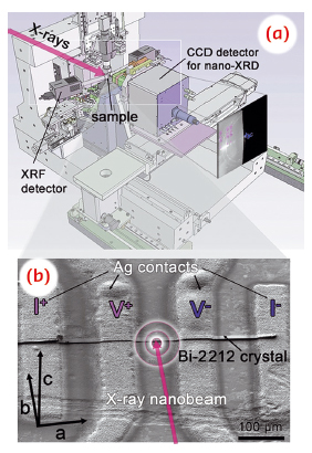
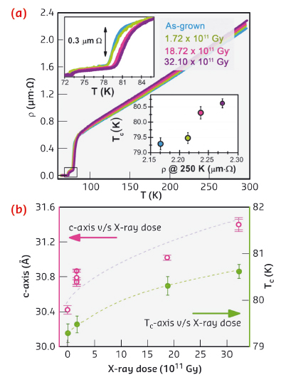
In particular, we investigated the effect of localised hard X-ray irradiation of Bi-2212 micro-crystals using the 117 × 116 nm2 nanoprobe available at the ID22NI beamline (now at ID16B) (Figure 59a). The structural modifications induced by the X-ray nanobeam were monitored using nano-XRD, while the corresponding changes in the electrical properties were measured by the four-probe method (Figure 59b) after each irradiation session. We have clearly proven that irradiating this material by 17 keV X-rays (doses in the order of 1012 Gy) results in an elongation of the c-axis and in an increase of both the critical temperature and the normal state resistivity (Figure 60). This highlights a modification in the material’s oxygen doping level, moving from an over-doped state towards a progressively more under-doped state.
 |
|
Fig. 59: a) Scheme of the experimental setup used at beamline ID22NI (now at ID16B). b) SEM micrograph of the typical chip used for electrical measurements of the Bi-2212 micro-crystals. Current and voltage electrodes used for the four-probe technique are labelled as I+, I-, V+ and V-. The arrow indicates the nanobeam direction during irradiation. |
 |
|
Fig. 60: a) Four-probes ab-plane resistivity vs. temperature curves for Bi-2212 micro-crystals in as-grown conditions and after increasingly higher X-ray doses. The insets report a magnification of the transition region and the Tc vs. resistivity dependence at room temperature. b) Dependence of the c-axis length and of the Tc on the X-ray dose. |
Moreover, modelling our different experimental conditions using the finite element method (FEM) allowed us to exclude heating induced by the X-ray nanobeam as the major cause for the change in the doping level. Conversely, a significant role could be played by the photoelectrons acting as a possible source of knock-on for the O atoms in the BiO layers, due to their low displacement threshold energy, which has already been predicted for the O atoms in the CuO chains of YBCO [4].
Our results suggest that the use of hard X-rays as a novel direct-writing, photoresist-free lithographic process is an attractive possibility to overcome the current limitations in the fabrication of miniaturised devices with potential nanometric resolution and 3D capability.
Principal publication and authors
A. Pagliero (a), L. Mino (b), E. Borfecchia (b), M. Truccato (a), A. Agostino (b), L. Pascale (b), E. Enrico (c), N. De Leo (c), C. Lamberti (b, d), and Gema Martínez-Criado (e), Nano Lett. 14, 1583 (2014).
(a) Depart. of Physics, NIS Centre of Excellence, University of Turin, Torino (Italy)
(b) Depart. of Chemistry, NIS Centre of Excellence, University of Turin, Torino (Italy)
(c) INRIM, National Institute of Metrological Research, Torino (Italy)
(d) Southern Federal University, Rostov-on-Don (Russia)
(e) ESRF


