- Home
- Users & Science
- Scientific Documentation
- ESRF Highlights
- ESRF Highlights 2015
- X-ray nanoprobe
- Coherent diffraction imaging of inversion domain boundaries
Coherent diffraction imaging of inversion domain boundaries
The first study of the displacement field induced by several inversion domain boundaries in gallium nitride (GaN) wires is reported here. A spatial resolution better than 10 nm and a displacement accuracy of a few picometres was achieved.
Nitride materials have been studied intensively and mastering their growth has opened the way to blue-light emission [1] and applications in power devices. Since defects in GaN wires are a key issue, their study can give new insight into the optoelectronic properties of nitride semiconductors.
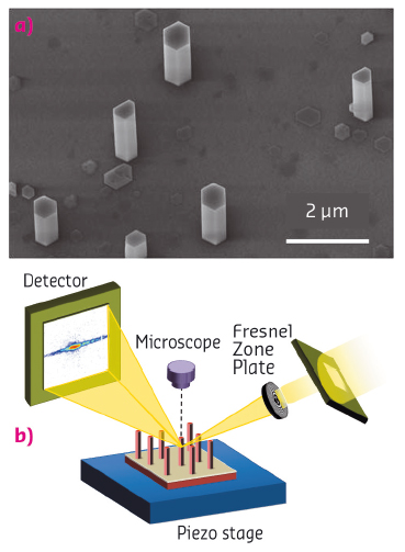
GaN wires were grown by metal organic vapour phase epitaxy on a c-oriented sapphire substrate (Figure 6a). They have their c-axis parallel or antiparallel to the growth axis and smooth lateral {110}m-plane facets. The coherent Bragg imaging (CBI) technique was used to investigate the arrangement of the inversion domain boundaries inside the GaN wires and the displacement field generated by these defects (Figure 6b).
 |
|
Fig. 6: (a) Scanning electron microscopy images of GaN wires. (b) Experimental setup at beamline ID01. |
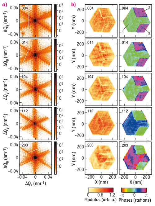
When a crystal is fully illuminated by a coherent X-ray beam, the scattered waves from all parts of the sample interfere in the diffraction pattern. The intensity scattered by the sample is measured in the far field and a real space image of the sample may be reconstructed from the intensity pattern thanks to phase retrieval algorithms [2]. The modulus M(r) and the phase Φ(r) of the reconstructed objects will be displayed in two separate images. M(r) is related to the electron density and Φ(r) includes the effects of the structure factors and the displacement field. Each Bragg peak is sensitive to the displacement field U(r) projected onto the scattering vector G, i.e. G.U(r). In this work, X-ray measurements were performed at beamline ID01. We measured five Bragg peaks: 004, 014, 104, 112 and 203. In all three-dimensional diffraction patterns, the measured intensity is concentrated in a (h,k)-plane perpendicular to the l-axis. This means that the inner structure of the measured slab is constant along the wire axis. 2D intensity maps were thus extracted from the 3D data sets in order to reconstruct a 2D image of the sample (Figure 7).
 |
|
Fig. 7: Coherent X-ray diffraction measurements of five Bragg reflections (a) and the corresponding real space reconstructions (b). |
The reconstructions (Figure 7b) clearly provide evidence of three domains: one large (1) and two small ones (2-3). The phase values are constant inside the domains and the two small domains show the same phase value for all reconstructions.
The homogeneity of the phase inside the domains denotes the absence of significant strain variation. The phase difference between the domains originates in the phase difference of the structure factor between Ga and N-terminated GaN domains and a homogeneous displacement of the domains between each other. One has to introduce a rigid displacement of the atomic lattice in the z direction of (c/2+8) pm of the +c with respect to the -c domains to match the experimental values. The error bar of this value is estimated to be 1 pm from the accuracy of the phase shift. It is possible to assert that the largest domain is -c (N-terminated) and the two small domains are +c (Ga-terminated), in agreement with the usual tendency of this type of wire growth.No displacement is needed to fit the experimental phase values in the (x,y)-plane. Nevertheless, the accuracy of the displacement in this plane is lower than the one along the z axis. It is estimated as 4 pm.
These values differ from those calculated for an isolated defect in an infinite media by Northrup et al. [3]. Interestingly, our molecular statics calculations with Tersoff-Brenner potential failed to reproduce the displacement field found experimentally, even though the complex configuration of domains had been taken into account.
In conclusion, this study demonstrates that the CBI technique offers a very precise inner view of the microstructure of small crystals in the presence of interacting defects. This technique can be also applied in a straightforward manner to materials under complex environment or operando as found in microelectronics and optoelectronics devices.
Principal publication and authors
S. Labat (a), M.-I. Richard (a,b), M. Dupraz (c,d), M. Gailhanou (a), G. Beutier (c,d), M. Verdier (c,d), F. Mastropietro (a), T.W. Cornelius (a), T.U. Schülli (b), J. Eymery (e,f) and O. Thomas (a), ACS Nano 9, 9210–9216 (2015); doi: 10.1021/acsnano.5b03857.
(a) Aix Marseille Univ., CNRS, Univ. Toulon, IM2NP UMR 7334, Marseille (France)
(b) ESRF
(c) Univ. Grenoble Alpes, SIMAP (France) (d) CNRS, SIMAP, Grenoble (France)
(e) Univ. Grenoble Alpes (France)
(f) CEA, INAC-SP2M, “Nanophysique et semiconducteurs” group, Grenoble (France)
References
[1] S. Nakamura et al., Jpn. J. Appl. Phys. 34, L797-L799 (1995).
[2] M.A. Pfeifer et al., Nature 442,63-66 (2006).
[3] J.E. Northrup et al., Phys Rev. Lett. 77,103-106 (1996).


