- Home
- Users & Science
- Scientific Documentation
- ESRF Highlights
- ESRF Highlights 2015
- X-ray nanoprobe
- Probing the strain in germanium nanowires by Laue microdiffraction
Probing the strain in germanium nanowires by Laue microdiffraction
The band structure of germanium can be tuned by application of very large stresses, which is only possible at the microscale. Probing both the strain state and the electro-optical properties on the same nano-object is a difficult challenge tackled here using synchrotron radiation.
Silicon and germanium are the most commonly employed materials in electronics. However, they are not key players in the world of emitter photonics materials since they are poor light emitters due to the indirect nature of their bandgaps – as compared to group III-V semiconductors which are not CMOS compatible. Yet germanium possesses a direct bandgap that is slightly (140 meV) above its fundamental (and indirect) bandgap. This peculiar feature, compared to silicon, has recently generated a great interest in the band diagram tailoring of germanium by application of very large strains. Indeed, tensile strain reduces the difference between the indirect and direct bandgaps [1] and can be used as a way to activate direct optical transition, a prerequisite to get a germanium based laser. It is thus necessary to correlate the strain state and the band diagram properties for the same microsized object. The latter has motivated this study on the effect of longitudinal stresses on the position of the direct bandgaps in germanium nanowires, which give the unique opportunity to probe the influence of stresses along the <111> crystallographic axis. Laue X-ray diffraction at beamline BM32 appeared to be the technique of choice to measure the deviatoric strain tensor in our nanowires.
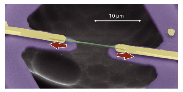
We grew the nanowires in a chemical vapor deposition (CVD) reactor using the vapor-liquid-solid mechanism [2]. The nanowires were then transferred by sonication onto a silicon nitride stressed layer on a silicon substrate. They were then encapsulated in a silicon oxide layer in order to mechanically anchor them on the nitride layer. We patterned the shape of two arms by lithography by aligning the lithographic mask on a nanowire. Finally, the nanowires were mechanically stretched by etching the silicon substrate underneath. The stretching arms retracted upon release, transmitting their elongation to the nanowire. Figure 24 shows a SEM image of such a stressed nanowire.
 |
|
Fig. 24: SEM image of a stressed germanium nanowire (in green). The silicon nitride is in purple and the gold contacts in yellow. |
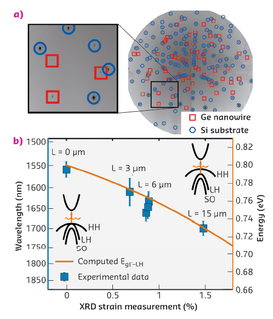
We accessed the strain components of such a system by Laue micro-diffraction. The white X-ray beam resulting from the bending magnet was focused onto a 300 nm x 300 nm spot and aligned at the centre of the nanowire. The resulting diffraction pattern was collected on a 2D detector at 90° from the incident beam, the sample being at 40°. Figure 25a shows a diffraction pattern from a strained germanium nanowire. Both nanowire and substrate X-ray diffraction patterns were measured. By removing the silicon background, we were able to obtain the orientation and the deviatoric strain tensor of the germanium nanowire – all strain components except the hydrostatic part. Assuming no stress on surfaces perpendicular to the axis of the nanowire, we were able to calculate a longitudinal strain up to 1.48% in the most stressed nanowire.
We finally measured the value of the light-hole band to Γ conduction band optical transition – one of the two direct bandgaps – by photocurrent spectroscopy. We excited the nanowire at different wavelengths using a Xe arc lamp and a monochromator. The generated electrical current – of about 200 fA – was probed using a lock-in amplifier. The obtained bandgaps were plotted as a function of strain measured by X-ray diffraction and compared to theoretical models from the literature [3], as shown in Figure 25b. A good agreement was observed.
 |
|
Fig. 25: (a) X-ray diffraction pattern of a single nanowire (b) Strain measurements compared with photocurrent spectroscopy bandgap measurements. |
In conclusion, we propose a novel approach to stress individual nano-objects (such as semiconducting nanowires, quantum dots in nanowires, nanotubes, etc.), using standard microfabrication processes. For the same single object, we have correlated the strain state and the band structure properties by using a combination of X-ray microdiffraction and microphotocurrent spectroscopy.
Principal publication and authors
Tensile strained germanium nanowires measured by photocurrent spectroscopy and X-ray microdiffraction, K. Guilloy (a), N. Pauc (a), A. Gassenq (a), P. Gentile (a), S. Tardif (b), F. Rieutord (b) and V. Calvo (a), Nano Lett. 15, 2429 (2015); doi: 10.1021/nl5048219.
(a) SINAPS, INAC-SP2M, Université Grenoble Alpes and CEA, Grenoble (France)
(b) NRS, INAC-SP2M, Université Grenoble Alpes and CEA, Grenoble (France)
References
[1] P. Boucaud et al., Photon. Res. 1, 102 (2013).
[2] R.S. Wagner and W.C. Ellis, Appl. Phys. Lett. 4, 89 (1964).
[3] C.G. Van de Walle, Phys. Rev. B 39, 1871 (1989).


