- Home
- Users & Science
- Scientific Documentation
- ESRF Highlights
- ESRF Highlights 2016
- X-ray nanoprobe
- Perovskite solar cells under the nXRD microscope
Perovskite solar cells under the nXRD microscope
A new technique based on scanning nanofocus X-ray diffraction paves the way for a better understanding of the links between crystal structure and morphology of the perovskite photo-active layer employed in third-generation solar cells.
At present, non-concentrator crystalline silicon technology dominates the photovoltaic (PV) industry with 25% record efficiency. In the past two decades, several next generation photovoltaic technologies have tried to compete with the silicon PV or attempted to occupy a position in niche PV markets. These technologies rely on photoactive materials that can be two orders of magnitude thinner than crystalline silicon, they can be printed or sprayed on flexible substrates using inexpensive methods, and some of them are as abundant as silicon. The first perovskite solar cell (PSC) was fabricated in 2009 and since then organic-inorganic hybrid PSCs have shown impressive progress, with record solar cells now achieving an astonishing certified 22.1% power conversion efficiency (PCE) [1]. This suggests that perovskites could be able to eventually replace standard crystalline silicon solar cells.
Fine control over the morphology and the crystallinity of thin film perovskites is vital to further improving the PCE. We have developed a technique based on a highly-focussed synchrotron X-ray beam to simultaneously probe the morphology and the structural properties of spin-coated mixed lead halide perovskite films for photovoltaic devices.
So far, the most widely employed techniques to investigate the crystal structure and morphology of perovskite films have been scanning microscopy and X-ray diffraction (XRD) techniques. With scanning microscopy methods such as scanning electron microscopy (SEM), distinguishing and isolating single perovskite crystallites in a ‘messy’ polycrystalline film is a difficult task. A further limitation is that these techniques are surface-sensitive, with the bulk of the material being essentially inaccessible. Synchrotron XRD methods such as grazing-incidence small- and wide-angle scattering (GI-WAXS and GI-SAXS) have been effectively employed to follow the structural evolution of perovskite films [2]. But in this case, typical X-ray beam sizes of hundreds of micrometres illuminate a large film area, and were therefore not small enough to examine the variation in the structural properties of the perovskite material across the sample.
 |
|
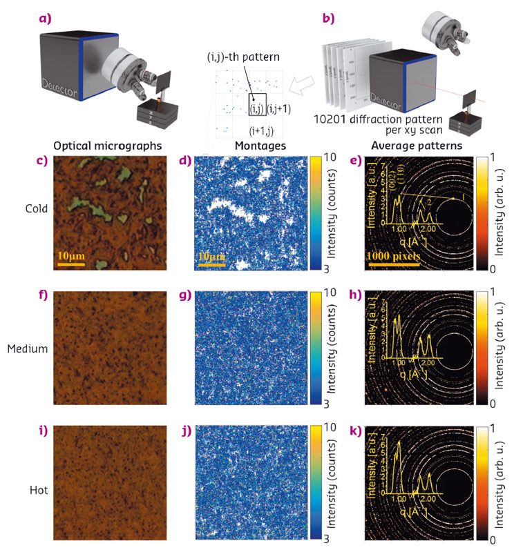
Fig. 46: Summary of measurements performed with scanning nanofocus XRD (nXRD) on perovskite films spin-coated with the substrate held at different temperatures: cold (room temperature), medium (~75°C), and hot (~90°C). a) nXRD scan area selection with the optical microscope. b) Setup during nXRD measurements. c, f, i) 40 × 40 μm2 optical micrographs acquired before the scan on the scan area for the cold, medium, and hot samples. d, g, j) 40 × 40 μm2 nXRD montages for the cold, medium, and hot sample. e, h, k) Average diffraction patterns recorded from the cold, medium, and hot sample (from doi: 10.1002/adfm.201603446). |
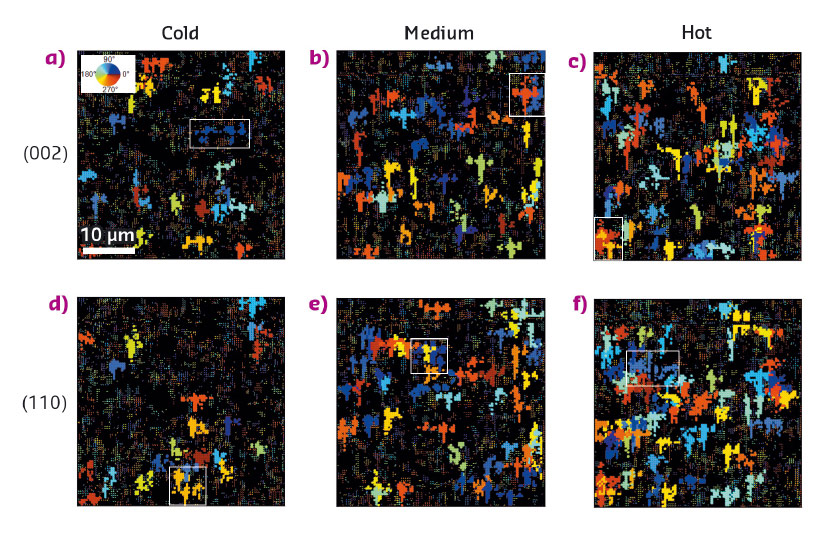
We overcame these limitations by employing a highly-focussed synchrotron X-ray beam at beamline ID13. We were able to raster scan an X-ray 'nanobeam' across a sample, and thus combine real-space imaging with sub-nanoscale structural information from XRD (see Figure 46). This allowed single perovskite grains buried within a complex, polycrystalline film to be selectively isolated and structurally characterised (see Figure 47).
 |
|
Fig. 47: 40 × 40 μm2 quiver plots highlighting (002) and (110) perovskite grains larger than 4 μm2. In a quiver plot, the value of one or more (002) or (110) diffraction spot peak angle (χp) is represented using an arrow with its centre located in the spatial position where the diffraction spot was acquired, and with an orientation and colour corresponding to χp. As the plots are resized for visualisation purposes, the arrows appear as single pixels. Clusters of pixels having the same colour represent single grains having the same orientation χp. The white boxes indicate the largest grains. Grains with different χ orientations are coloured in a different way according to the colourmap shown in inset in (a) (from doi: 10.1002/adfm.201603446). |
With nXRD, we were able to perform grain segmentation and extract the lateral size, strain and orientation of individual perovskite platelets. The technique was employed to determine information such as surface coverage and grain statistics from perovskite films that were spin-coated on substrates, held at different temperatures and subsequently employed in the fabrication of high performance solar cells. Films coated on substrates held at relatively high temperatures were found to have a lower density of pinholes and larger grain size.
This technique could be used to characterise a range of new perovskite materials and develop detailed models that relate their complex nano-morphology to their optical and electronic properties. We are already looking forward to future experiments at ID13 in the attempt to combine nXRD with in situ growth and crystallisation processes in real-time.
Principal publication and authors
Mapping morphological and structural properties of lead halide perovskites by scanning nanofocus XRD, S. Lilliu (a), T.G. Dane (b), M. Alsari (c), J. Griffin (a), A.T. Barrows (a), M.S. Dahlem (d), R.H. Friend (c), D.G. Lidzey (a) and J.E. Macdonald (e), Advanced Functional Materials (2016); doi: 10.1002/adfm.201603446.
(a) Department of Physics and Astronomy, University of Sheffield (UK)
(b) ESRF
(c) Cavendish Laboratory, University of Cambridge (UK)
(d) Masdar Institute of Science and Technology, Abu Dhabi (UAE)
(e) Cardiff University (UK)
References
[1] NREL. Efficiency Chart, http://www.nrel.gov/ncpv, accessed 8 Oct 2016.
[2] A.T. Barrows et al., Advanced Functional Materials 26, 4934-4942 (2016); doi: 10.1002/adfm.201601309.


