- Home
- News
- Spotlight on Science
- X-ray techniques...
X-ray techniques investigate copper doping processes in zinc-oxide nanowires
07-02-2025
X-ray absorption spectroscopy at beamline ID12 was employed to investigate copper doping in zinc-oxide nanowires for piezoelectric devices. Approximately 15% of the copper formed CuZn dopants, while the majority remained at the surface. Thermal annealing in an O₂ atmosphere activated CuZn-VZn defect complexes, increasing electrical resistivity and enhancing emission properties. These findings improve the understanding of compensatory doping, contributing to the optimization of ZnO-based devices.
Share
The development of wurtzite ZnO nanowires as biocompatible and sustainable semiconductors at the nanoscale has attracted increasing interest in electronics and energy applications [1]. A widely explored piezoelectric device involves vertically integrating ZnO nanowires between two electrodes to harvest ambient mechanical energy as a micro-source of power. However, the screening of the piezoelectric potential generated under mechanical stress remains a significant challenge, hindering performance.
This screening effect results from the high density of free electrons in ZnO nanowires, primarily due to the incorporation of hydrogen-related defects during their growth via chemical bath deposition [2]. Efforts to mitigate this issue have focused on reducing hydrogen-related defects through post-deposition treatments [3], but their impact on piezoelectric performance has been limited.
A more promising approach involves introducing Cu dopants as acceptors into ZnO nanowires, employing compensatory doping to reduce the free electron density. The effectiveness of this strategy depends critically on the local positions and environments of the Cu dopants, which were previously not fully understood.
This study examined the incorporation of Cu into ZnO nanowires by combining X-ray absorption near-edge structure (XANES) spectroscopy with mass spectrometry and optical spectroscopy. ZnO nanowires were grown by chemical bath deposition with varying Cu dopant concentrations and subsequently subjected to thermal annealing at 500°C for one hour in an O2 atmosphere. The samples were analyzed using X-ray linear dichroism (XLD) at beamline ID12 at the Zn and Cu K-edges to probe the local positions and environments of the Cu dopants in the ZnO nanowires.
The experimental Zn K-edge XANES spectra for Cu-doped ZnO nanowires with a [Cu]/[Zn]bath ratio of 5% are presented in Figures 1a and 1b. The spectra were recorded with the polar c-axis oriented perpendicular (E⊥c) and parallel (E//c) to the electric field of the linearly polarized X-ray beam, with their difference represented as the XLD spectrum. The XANES and XLD spectral shapes confirm that Zn atoms maintain a 2+ oxidation state and adopt the characteristic wurtzite configuration of ZnO nanowires, where Zn2+ cations are tetrahedrally coordinated by O2- anions.

Click figure to enlarge
Fig. 1: a) Zn K-edge XANES and (b) corresponding XLD spectra of Cu-doped ZnO nanowires grown by chemical bath deposition (CBD) with a [Cu]/[Zn]bath ratio of 5%. c) Normalized Cu K-edge XANES and (d) corresponding XLD spectra of ZnO nanowires grown by CBD with [Cu]/[Zn]bath ratios of 1%, 3%, 5% and 10%. e) Normalized Cu K-edge XANES and (f) corresponding XLD spectra of ZnO nanowires grown by CBD with a [Cu]/[Zn]bath ratio of 5%, recorded before and after thermal annealing at 500°C for one hour under an O2 atmosphere.
The normalized isotropic Cu K-edge XANES and corresponding XLD spectra of ZnO nanowires grown at different [Cu]/[Zn]bath ratios are shown in Figures 1c and 1d. The isotropic XANES spectra maintain a consistent shape across all [Cu]/[Zn]bath ratios, featuring a leading-edge peak followed by a prominent feature approximately 11 eV higher. No pre-edge peak is observed above the noise level. The XLD spectra at the Cu K-edge closely resemble those at the Zn K-edge, exhibiting minimal dependence on the [Cu]/[Zn]bath ratio. This similarity indicates that only a minority of Cu atoms adopt a wurtzite configuration by substituting Zn sites as CuZn dopants. By comparing the XLD intensities at the Cu and Zn K-edges, it was determined that only 15 ± 5% of the total Cu is incorporated as CuZn, while the majority (~85%) exists in a Cu2O-like environment, primarily located on the nanowire surface.
Following thermal annealing of the Cu-doped ZnO nanowires, notable changes were observed in the isotropic XANES and XLD spectra at the Cu K-edge, as shown in Figures 1e and 1f. The isotropic XANES spectra show the disappearance of the sharp peak at the leading edge, accompanied by broadening of the subsequent prominent peak. In the XLD spectra, a moderate peak emerges around 9890 eV, while the most intense peak at ~9000 eV shifts slightly (~2 eV) to higher energies. These spectral modifications indicate a change in the electronic structure of the Cu dopants, suggesting a more oxidizing local environment and the formation of VZn defects near Cu atoms.
The combination of XANES and XLD with mass spectrometry, optical spectroscopy, and electrical measurements facilitated the estimation of CuZn dopant concentrations ranging from 1.3 to 12.7 x 10¹⁷ at/cm3. This approach also enabled the correlation of the zero-phonon line emission, strongly coupled with phonons at 2.86 eV, to CuZn-VZn complexes. Additionally, the electrical activity of the CuZn-VZn defect complexes was identified, as illustrated in Figure 2.
Click figure to enlarge
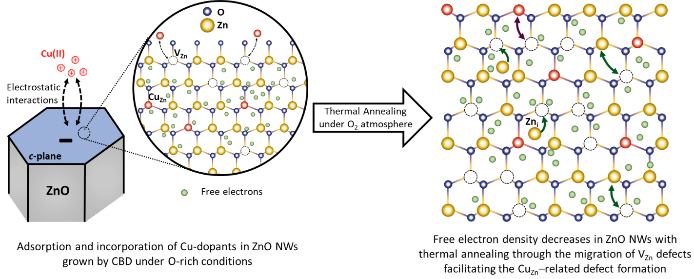
Fig. 2: Schematic representation of the adsorption and incorporation processes of Cu atoms in ZnO nanowires grown by CBD in a high-pH environment. The figure also illustrates the migration of CuZn acceptors, facilitated by the extensive formation and diffusion of VZn defects following thermal annealing at 500°C under an O2 atmosphere.
These findings offer new insights into the incorporation of Cu into ZnO nanowires and highlight the importance of thermal activation in forming electrically active CuZn-VZn defect complexes. The next step will focus on increasing the content of Cu dopants, effectively promoting CuZn formation rather than having the majority of Cu accumulate on the surfaces of ZnO nanowires. This work opens new perspectives for drastically reducing the detrimental screening of piezoelectric potential through compensatory doping and, consequently, for improving the power density of ZnO nanowire-based piezoelectric devices.
Principal publication and authors
Incorporation and Compensatory Doping Processes of Cu into ZnO Nanowires Investigated at the Local Scale, M. Manrique (a,b,c), B. Salem (b), E. Sarigiannidou (a), H. Roussel (a), F. Wilhelm (d), F. Donatini (e), V. Jacob (f), G. Le Rhun (c), V. Consonni (a), Small Struct., 2400534 (2024); https://doi.org/10.1002/sstr.202400534
(a) Université Grenoble Alpes, CNRS, Grenoble INP, LMGP, Grenoble (France)
(b) Université Grenoble Alpes, CNRS, CEA, Grenoble INP, LTM, Grenoble (France)
(c) Université Grenoble Alpes, CEA, LETI, Grenoble (France)
(d) ESRF
(e) Université Grenoble Alpes, CNRS, Grenoble INP, Institut NEEL, Grenoble (France)
(f) Université Grenoble Alpes, CNRS, IRD, Grenoble INP, IGE, Grenoble (France)
References
[1] R.K. Pandey et al., J. Phys. D: Appl. Phys. 4, 044011 (2021).
[2] J. Villafuerte et al., J. Phys. Chem. C 124, 16652-16662 (2020).
[3] J. Villafuerte et al., Phys. Rev. Mater. 5, 056001 (2022).
| About the beamline: ID12 |
|
Beamline ID12 specializes in polarization-dependent X-ray spectroscopy within the tender and hard X-ray range (2 -15keV), offering full control over the polarization state of the X-ray beam. Its research activities focus on investigating the electronic and magnetic properties of diverse systems, ranging from bulk permanent magnets and diluted magnetic semiconductors to paramagnetic monolayers on surfaces, with element- and orbital-selective sensitivity. A wide array of dichroic experiments can be performed, probing magnetism, chirality, or both, under extreme conditions, including magnetic fields up to 17 T, temperatures spanning from 2K to 800K, and pressures reaching 60 GPa. The beamline’s exceptional optical stability, combined with a highly efficient detection system, enables the reliable measurement of dichroic signals with an unprecedented signal-to-noise ratio. Using a focused ESRF-EBS beam, twin domain mapping in chiral systems can be conducted with micrometric resolution. Additionally, the ULMAG setup allows users to perform X-ray magnetic circular dichroism, X-ray diffraction, and bulk property measurements – including magnetization, magnetostriction, magnetocalorics, and magnetoresistance – under strictly identical experimental conditions. This unique and versatile tool provides crucial insights into the interplay between magnetic, structural, and electronic subsystems in a wide range of magnetic materials. |
partners


European Synchrotron Radiation Facility - 71, avenue des Martyrs, CS 40220, 38043 Grenoble Cedex 9, France.