- Home
- News
- General News
- A new technique...
A new technique to see crystals like never before
29-11-2011
An international team of scientists led by the Fresnel Institute (CNRS/University of Central Aix-Marseille/Ecole Marseille) and the ESRF has developed a new technique to make visible nanometre-sized structures in crystalline materials. This technique combines two pioneering approaches in nanocharacterisation: lensless microscopy and scanning X-ray diffraction microscopy. The image of the nano-structured object is quantitative, three-dimensional and of high-resolution. The technique could revolutionise research in various disciplines where complex crystal structures are studied, such as the life sciences and microelectronics. The work is published in the journal Nature Communications dated 29 November 2011.
Share
Jointly published by the CNRS and the ESRF.
To date, two techniques have been used to analyse complex crystalline materials, each having specific limitations. Classic "X-ray diffraction" can acquire information on atomic positions and irregularities in the sample without damaging the sample, but with a limited spatial resolution in the range of a micrometre. Transmission electron microscopy (TEM) exhibits a much better spatial resolution (0.1 nm), providing a "real" image of the crystal, but has the disadvantage that the sample is destroyed in the process.
The new technique developed by Virginie Chamard (CNRS) of the Institute Fresnel and her colleagues overcomes these limitations by combining the advantages of both methods: it produces high-resolution 3D images – down to a few tens of nanometres - without destroying the sample, and it provides as much information as conventional X-ray diffraction on the atomic structure. In addition, it enables analysis of very large areas, potentially of infinite dimensions.
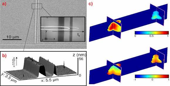
The new technique uses a microscopic beam of X-rays produced by a synchrotron—for their work, researchers used ESRF beamline ID01—and focuses it on the sample. This lens-less microscopy technique, where computers replace the lens, exploits the coherence properties of the X-ray beam. As the beam scans across the sample, a detector captures the diffracted X-rays and acquires a series of "diffraction patterns". These are processed by a special algorithm generating a 3D image of the entire sample with a resolution smaller than the width of the X-ray beam.
The foundations of this technique called "ptychography" were laid in 1969 by German physicist Walter Hoppe who invented it to improve the resolution of electron microscopy. Virginie Chamard and her team spent three years developing the technique for the imaging of crystals.
This new microscopy approach could be crucial to our understanding of many mysteries both scientific and technological, for example the growth of mollusk-shells and the optical properties of semiconductors. It could even help in studies to improve the electrical performance of metal alloys. These examples all involve complex crystalline materials, for which the new technique was specifically developed.
Reference
Three-dimensional high-resolution quantitative microscopy of extended crystals, P. Godard et al., Nature Communications, November 29, 2011.
Top image: Ptychography scan of lines patterned on a silicon-on-insulator substrate.


