- Home
- News
- Spotlight on Science
- The compliant behaviour...
The compliant behaviour of germanium nanocluster arrays on free-standing silicon nanostructures
09-01-2012
“Don’t change a winning team” is a widely known sport paradigm on short-term success. However, it is also evident that success on the long-term is no longer guaranteed when teams do not further develop. In this respect, a coach must sooner or later answer the question how to integrate a new “high potential” player into a winning team, guaranteeing the optimal use of his high performance while conserving simultaneously the enthusiastic team spirit. Certainly, this is only possible when both sides – team & candidate – respect each other and face each other in a flexible way.
Share
Materials scientists in silicon microelectronics face a very similar task. Silicon, dominating the platform for integrated circuitry technologies over the last 50 years, is running into fundamental physical limits with further miniaturisation (“More Moore”) and/or functionalisation (“More than Moore”). In this respect, suitable material candidates must be identified to enable new innovative functions without compromising the high performance of the silicon chip baseline technology. For the integration of photonics modules in silicon microelectronics, materials scientists from the Leibniz Institute of Innovative Microelectronics (IHP) in Frankfurt/Oder (Germany) developed an 8” silicon wafer process to selectively grow germanium nanocrystals by chemical vapour deposition on an array of free-standing Si nanopillar structures of about 40 to 50 nanometres (nm) in diameter [1]. The high potential of Ge for photonic applications [2-4] lies in its superior optoelectronic properties such as band gap and charge carrier mobility. Despite clear advantages of Ge integration in Si technology (identical diamond crystal structure with Si, CMOS compatibility due to the absence of contamination risks, etc.), it faces also some real challenges limiting the optoelectronic performance. Among them, thermal and lattice mismatch result in too high defect levels (which act as non-radiative recombination centres). Parasitic diffusion and formation of SiGe alloys at elevated temperatures is also a common problem. In this respect, Ge heteroepitaxy approaches must be developed for high quality Ge nanostructure growth with reasonable thermal budget.
High strain energy resulting in defect generation is a problem that needs to be overcome. In classical Ge heteroepitaxy on bulk Si substrates, the strain accumulated only in the epilayer is relieved by defect formation beyond the so-called critical thickness [5]. In other words, the classical approach does not allow a successful introduction of the new “promising player Ge” to the winning “Si team” so that its potential for high performance cannot be fully exploited. The compliant behaviour of Ge/Si nanostructures, however, offers a promising vision: In contrast to the classical Ge deposition on bulk Si substrates, the strain energy accumulated in the Ge epilayer is partially shifted to the free-standing Si nanostructure [6]. This strain partitioning phenomenon is at the very heart of the compliant substrate effect and, if strain energy levels are correctly balanced, offers the vision to grow defect-free nanostructures of lattice mismatched semiconductors on Si. In the case of the Ge/Si heterosystem with a lattice mismatch of 4.2%, the strain partitioning phenomenon is expected to be triggered when free-standing Si nanopillars with the challenging width of 50 nm and below are used.
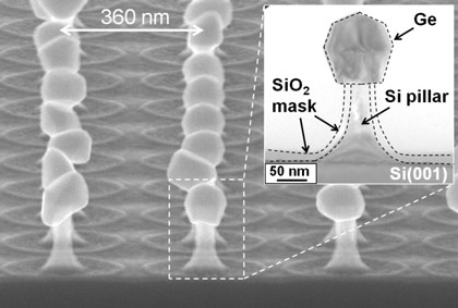
Such 50 nm wide Si nanopillars with selectively grown Ge nanoclusters were fabricated using a combined CMOS gate spacer process of the IHP 0.13 µm BiCMOS technology [7] and an isotropic wet etching. The growth selectivity was triggered by opening growth seeds in SiO2 protected nanopatterned Si substrate (see Figure 1). However, nanoscale free-standing Ge/Si nanostructures proved to be both challenging to fabricate and demanding to investigate. Therefore, material characterisation was performed using synchrotron based X-ray diffraction at the state-of-the-art ID01 beamline. The experiment was performed at an X-ray energy of 11 KeV in grazing incidence mode (0.15°) to provide high sensitivity towards Ge/Si nanostructures.
 |
|
Figure 1. Scanning and transmission electron microscope images of Ge nanoclusters on free-standing Si(001) nanopillars. |
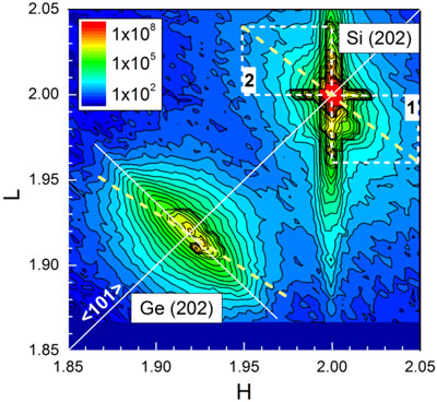
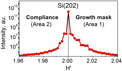
The strain in Ge/Si nanostructures was analysed by studying the diffuse scattering around the (202) Bragg reflection as shown in Figure 2. In particular, fingerprints of compliant substrate effects were examined along the Poisson line through the Si(202) signal (marked in the graph) and presented in Figure 3. Two regions of opposite strain behaviour in the in-plane direction can be found. Area 1 with a streak at H>2 and L<2 corresponds to a Si nanopillar compressed by the thermally grown SiO2 growth mask surrounding the nanostructure. Area 2 with a streak at H<2 and L>2 reflects, on the other hand, Si tensile-strained by the overgrowing Ge epilayer and thus reflects its potential compliant character. This effect is, however, limited and the Si nanopillar is mainly affected by SiO2. Despite the absence of the strain partitioning phenomenon between Ge and Si, the position of Ge(202) Bragg reflection corresponds to a material with a bulk lattice constant. Thus the strain energy in the epilayer is relieved plastically via nucleation of misfit dislocations at the Ge/Si interface. Transmission electron microscopy studies [1] show that Ge nanoclusters with no additional volume defects and thus of high quality can be achieved by this technique.
 |
|
Figure 2. Reciprocal space map around (202) Bragg reflections of Ge and Si. Dashed yellow lines depict the Poisson line. |
In conclusion, our approach using the compliant substrates theory provides an interesting method of integrate high quality lattice mismatched semiconductors into main stream Si microelectronics to enable higher performance and/or new functions. However, the theory does not yet include important aspects of thin film growth on the nanoscale: using the example of the Ge/Si heterosystem, the theory is focused on the nanostructure properties alone but does not yet include the influence of the surrounding environment (which is however required in the complex processing and growth procedure). In particular, in the present study, it is the stress field exerted by the SiO2 growth mask on the Si nanostructure which limits its effectiveness to act as a compliant substrate during Ge nanostructure overgrowth. Whereas, turning back to our real-life scenario from sports, the flexibility of a “winning team” to welcome a new high potential team player does not only depend on the player's willingness and capabilities but also very much on the boundary conditions within which it is moving.
 |
|
Figure 3. Intensity along the Poisson line across the Si(202) Bragg reflection. |
Principal publication and authors
G. Kozlowski (a) , P. Zaumseil (a), M.A. Schubert (a), Y. Yamamoto (a), J. Bauer (a), J. Matejova (a,b), T. Schulli (c), B. Tillack (a,d), and T. Schroeder (a), Compliant substrate versus plastic relaxation effects in Ge nanoheteroepitaxy on free-standing Si(001) nanopillars, Appl. Phys. Lett. 99, 141901 (2011).
(a) IHP, Frankfurt/Oder (Germany)
(b) Charles University in Prague (Czech Republic)
(c) ESRF
(d) Technische Universität Berlin (Germany)
References
[1] G. Kozlowski et. al., Appl. Phys. Lett. 99, 141901 (2011).
[2] P. H. Lim et. al., Appl. Phys. Lett. 93, 041103 (2008).
[3] N. P. Stepina et. al., Appl. Phys. Lett. 98, 142101 (2011).
[4] J. Liu et. al., Optics Express 15, 11272 (2007).
[5] J. E. Ayers, Heteroepitaxy of Semiconductors: Theory, Growth and Characterization (Taylor & Francis Group) (2007).
[6] D. Zubia et. al., J. Appl. Phys. 85, 6492 (1999).
[7] H. Rücker et. al., Proceedings of IEEE BCTM, Capri, Italy, 13-14 October (IEEE, New York), 166-169 (2009).
Top image: Germanium nanoclusters on free-standing silicon nanopillars.


