- Home
- News
- Spotlight on Science
- X-ray excited optical...
X-ray excited optical imaging of nanosized light emitting diodes
24-10-2012
Direct observation of geometrical carrier localisation in single hexagonal core-multishell nanowires was used by researchers at the ESRF to demonstrate that size-dependent phenomena at the nanoscale can be imaged by X-ray excited optical luminescence. This research provides a glimpse of the potential that a hyperspectral imaging method can provide.
Share
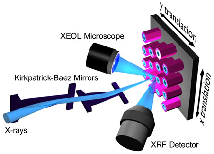
Imaging schemes capable of overcoming Abbe’s diffraction barrier (λ/2NA, where λ is the wavelength of light and NA is the numerical aperture of the lens) are revolutionising optical microscopy. A promising approach is based on the use of wavelengths shorter than those of visible light. Hard X-ray microscopy is particularly attractive for non-invasive optical imaging at the nanoscale thanks to the advent of X-ray focusing optics, which provides a nanosized excitation beam, and because of the quantum confinement effects in nanostructures, which limit the free carrier dynamics. So far, X-ray excited optical luminescence has been mostly a synchrotron soft X-ray technique that suffers from poor spatial resolution and long carrier diffusion length. Here we present an imaging scheme that combines X-ray excited optical luminescence [1] with simultaneous X-ray fluorescence using a nanometre-sized hard X-ray beam (Figure 1).
Although several exciting approaches in light imaging methods have emerged recently that can ‘‘break’’ the Abbe diffraction rule under certain circumstances [2], the use of nanometre-sized hard X-ray beams to generate light emission governed by size-dependent phenomena provides unique advantages over near-field imaging approaches (restricted to surfaces with small areas in the region within ~ 10 nm of the tip or nano-antennas), or far-field imaging techniques (that involve photoactivatable fluorophores). The underlying mechanisms allow us to create an imaging approach with simultaneous optical, chemical and spectral resolution at the nanometre scale.
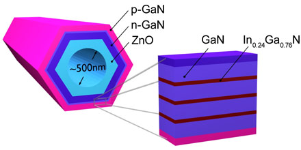
Core/multishell nanowires, which produce a variety of size-dependent phenomena for advanced light-emitting diodes, were used to validate the principles involved (Figure 2). Although theoretical calculations suggest that the carrier distribution in nanowires exhibits a two dimensional confinement under a cross-section of hexagonal geometry [3], its direct observation has never been addressed. Using a Kirkpartrick-Baez mirrors based X-ray nanoprobe with 60 x 60 nm2 spatial resolution at ESRF’s beamline ID22, we found experimental evidence of carrier localisation phenomena preferentially at the corners of hexagonal single coaxial n-GaN/InGaN multiquantum-well/p-GaN nanowires (Figure 2).
 |
|
Figure 2. Sketch of the p-GaN/In1-xGaxN/n-GaN/ZnO nanowire light emitting diode and magnified cross-sectional view highlighting the GaN/InGaN multi-quantum well. |
Matching theoretical predictions (Figure 3), our experiment narrows the gap between optical microscopy and high-resolution X-ray imaging, and calls for further studies on optoelectronic nanodevices and light emitting molecules in biological sciences. It represents a step towards not only the validation of theories of quantum confinement, but also the realisation of nanostructures with spectroscopic properties that could prove advantageous in light-emitting devices. Its great potential could be further enhanced by the addition of time resolution, or by using this technique in conjunction with other methods, such as X-ray absorption spectroscopy and X-ray diffraction at the nanoscale.
Principal publication and authors
Probing quantum confinement within single core-multishell nanowires, G. Martínez-Criado (a), A. Homs (a), B. Alén (b), J.A. Sans (c), J. Segura-Ruiz (a), A. Molina-Sánchez (d), J. Susini (a), J. Yoo (e), G.-C. Yi (e), Nano Letters (2012) in press.
(a) ESRF
(b) Instituto de Microelectrónica de Madrid (CNM, CSIC), Tres Cantos (Spain)
(c) MALTA Consolider Team, Universitat Politecnica de Valencia, Valencia (Spain)
(d) Institute for Electronics, Microelectronics, and Nanotechnology, CNRS-UMR 8520, Department ISEN, Villeneuve d’Ascq (France)
(e) National CRI Centre for Semiconductor Nanorods, Department of Physics and Astronomy, Seoul National University (Republic of Korea)
References
[1] A. Rogalev, J. Goulon, X-ray Excited Optical Luminescence Spectroscopies, Chemical Applications of Synchrotron Radiation Part II, World Scientific: Singapore (2002).
[2] D.K. Gramotnev, S.I. Bozhevolnyi, Nature Photon. 4, 83 (2010).
[3]B.M. Wong, F. Leonard, Q. Li, G.T. Wang, Nano Lett. 11, 3074 (2011).
Top image: Quantum confinement effects probed by XEOL on a single core-multishell nanowire.


