- Home
- News
- Spotlight on Science
- Three-dimensional...
Three-dimensional Si/Ge quantum dot crystals
24-01-2008
Semiconductor quantum dots are already being used for optoelectronic applications, exploiting the increased density of states and tuneable energy levels due to quantum confinement. So far, only the properties of single dots have been used. Here we show that for closely spaced dots, their energy levels couple, leading to the formation of an electronic band structure in a periodic dot arrangement.
Share
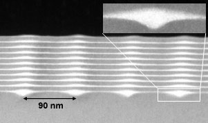
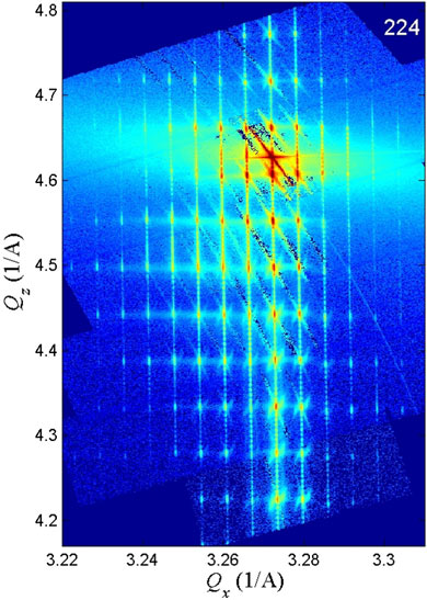
Semiconductor quantum dots have their name because their small size causes quantum confinement and creates specific electronic states. By controlling the material’s composition and the size and shape of the dots, their optoelectronic properties can be tuned, creating “artificial atoms”. For advanced devices, it would be interesting to couple such artificial atoms to create artificial molecules or even an artificial crystal. Our work concentrates on the latter, the creation of an artificial crystal, which requires a periodic arrangement of quantum dots with an extremely low scatter of properties in a single crystalline matrix. This was achieved using extreme ultraviolet interference lithography to create periodic pits in a Si(001) substrate. The lithography was carried out at the Swiss Light Source using multiple exposures to define a 2D periodic pattern with a period of 100×90 nm2. The pattern served as a template to grow first a 2D periodic SiGe dot layer by molecular beam epitaxy, which was subsequently overgrown by a Si/Ge multilayer. In the Ge layers, islands form exactly above the dots in the first layer due to elastic interactions, as shown in the TEM cross-section in Figure 1. The perfection of the 3D-periodic quantum dot crystal was obtained from the diffraction pattern in an X-ray diffraction experiment carried out at ESRF beamline ID10B (Figure 2). A series of satellite peaks along the growth direction and parallel to the surface shows the periodic arrangement of quantum dots. The electronic states have been calculated using the chemical composition and strain distributions derived from the XRD data, and are shown in Figure 3. It can be seen that while holes are located within the SiGe islands, electrons are confined in strained Si regions above/below and at the sides of the dots. These states of neighbouring dots couple and form extended states, i.e. an artificial band structure. Photoluminescence measurements are in very good agreement with these calculations.
 |
|
|
Figure 1: Transmission electron microscopy (TEM) image of 10 period stacks of Ge islands and Si spacer layers (10 nm) deposited on a pre-patterned area, demonstrating the vertical and the lateral ordering, which is maintained after 10 periods. |
Tuning the properties and distances of the quantum dot crystals, the coupling and hence the band structure can be controlled. Lateral periods down to 30 nm are feasible using the combination of extreme ultraviolet photolithography for substrate patterning and self-organised growth. This opens the way towards devices relying on coupled quantum dots, important for spintronics or solid-state concepts of quantum computing.
 |
|
Figure 2: Reciprocal space maps around the (224) Bragg peak taken from a three-dimensional Si-Ge quantum dot crystal with 10 periods. |
Principal publications and authors
D. Grützmacher (a,b), T. Fromherz (c), C. Dais (b), J. Stangl (c), E. Müller (b), Y. Ekinci (b), H.H. Solak (b), H. Sigg (b), R.T. Lechner (c), E. Wintersberger (c), S. Birner (d), V. Holý (e), G. Bauer (c), Three-Dimensional Si/Ge Quantum Dot Crystals, Nano Letters 7, 3150-3156 (2007).
(a) Forschungszentrum Jülich (Germany)
(b) Paul Scherrer Institut (Switzerland)
(c) Johannes Kepler University Linz (Austria)
(d) Walter Schottky Institut, Technical University Munich (Germany)
(e) Masaryk University, Brno (Czech Republic)


