- Home
- News
- Spotlight on Science
- Probing the mechanical...
Probing the mechanical properties of nano-sized objects by a combined in situ AFM and micro-XRD technique
16-07-2008
Investigation of the elastic response of nano-sized objects under external mechanical stress has been made possible thanks to a novel atomic force microscope (AFM), recently developed at the ESRF. When mounted on the diffractometer of beamline ID01, the AFM permits the in situ combination of AFM-techniques (both, imaging and indentation) and micro X-ray diffraction.
Share
Semiconductor nanostructures, strained during coherent growth on substrates, have been extensively investigated because of their potential application in new nanotechnology-based devices. While the elastic properties of bulk and thin films are well known, it is expected that the mechanical behaviour changes as the size of the material is reduced in 2 or 3 dimensions to the nanometre scale. Nano-indentation - i.e. applying an external localised force to a nano-sized object - and the in situ measurement of the related strain response by micro X-ray diffraction (µ-XRD) is the approach we have taken in a recent experiment at ID01.
A new in situ atomic force microscope has been developed during the X-Tip EU project and is now commercialised by Small Infinity. Using this AFM, we successfully positioned selected nanostructures on a substrate into the microfocused X-ray beam, which had a footprint of approximately 3 x 1.5 µm, and used the AFM-tip as an indenter. Figure 1 shows a schematic overview of the setup.
 |
|
Figure 1. Experimental setup, showing the scanning table of the AFM (left) and a schematic overview of the combined in situ AFM and the µ-XRD (right). |
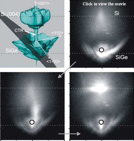
Two kinds of objects have been investigated, so-called semiconductor rolled-up nanotubes [1] and SiGe islands [2]. Here we report on the SiGe islands, which are grown by liquid phase epitaxy (LPE) in the Stranski-Krastanov growth mode. The resulting shape is a truncated pyramid with a base-length of about 1000 nm, and a height of 500 – 700 nm. The island’s average Ge concentration was 14%. Due to the shape of the island and its lattice parameter difference with the substrate, the 3D diffraction pattern close to the (004) reflection is rather complex, this is shown in Figure 2a. The slice recorded by the CCD detector results in a 2D projection of the intensity distribution. This slice is further used to follow the response of the island while it is being stressed by the AFM tip. A force applied by the AFM-tip can induce a compression of the SiGe-island’s lattice parameter perpendicular to the surface and thus a shift of the island’s diffuse scattering towards the (004) Si position. This can be clearly seen in the sequence of diffraction patterns in Figure 2. Note that the position of the substrate’s crystal truncation rod (CTR, circles in Figure 2) remains unchanged, indicating that the substrate’s orientation is not changed by the applied force. Two main features should be emphasised: i) From the shift of the SiGe peak, the lattice parameter compression can be followed until it reaches the level of the substrate (corresponding to about Δa/a=0.6%) and ii) While retracting the AFM-tip, the scattering signal follows back to it’s original position which indicates, that the deformation took place within the elastic regime. In the case of an experiment with rolled-up nanotubes, deformation in both, the elastic and plastic regime was observed.
By these pioneering experiments we have opened the door to studies of the influence of nanoscale dimensions on the elastic properties of materials.
 |
|
Figure 2. Scattering pattern of SiGe islands close to the Si (004) reflection. a) simulated 3D intensity distribution of the SiGe islands and the distorted Si substrate together with a 2D slice depicting the CCD-detector plane (dark grey). b-d) images demonstrating the change of the scattering signal during the process of indentation. The circles correspond to the position of the CTR. Clicking on the image will open a short video (AVI uncompressed) showing the changes in more detail including the elastic response during retraction of the tip. |
References
[1] B. Krause, C. Mocuta, T.H. Metzger, Ch. Deneke and O.G. Schmidt, Phys. Rev. Lett. 96, 165502 (2006).
[2] C. Mocuta, J. Stangl, K. Mundboth, T.H. Metzger, G. Bauer, I.A. Vartanyants, M. Schmidbauer, T. Boeck, Phys. Rev. B 77, 245425 (2008).
Authors
T. Scheler (a), M.S. Rodrigues (a), C. Mocuta (a), A. Malachias (a,b), O. Dhez (a), F. Comin (a), J. Chevrier (c) and T.H. Metzger (a).
(a) ESRF, Grenoble (France)
(b) MPI f. Festkörperforschung, Stuttgart (Germany)
(c) Institut Néel, CNRS/UJF, Grenoble (France)


