- Home
- News
- Spotlight on Science
- Individual GaAs...
Individual GaAs nanorods imaged by coherent diffraction
03-04-2009
Visualising nanoscale objects can be a challenge. Scientists have succeeded in using coherent X-ray diffraction to examine in detail nanorods grown in an array using a pre-patterned substrate. Their results shed light on local effects in the growth of such nanorods.
Share
Semiconductor nanorods have potential to provide us with new materials possessing unusual electronic and optical properties [1]. This may include integrated devices like vertical FET transistor arrays with ultra-high carrier density or LEDs. Heterostructures of materials with a large lattice mismatch can be created using the nanorod approach. In combination with quantum-confinement effects of charge carriers in the nanorods, these devices offer novel possibilities for bandgap-engineering.
Catalyst-assisted growth techniques are widely used for the fabrication of nanorods. Such methods are not ideal because of the random position of the nanorods on the surface and the strong variation in the diameter of the nanorods. This hinders, for example, creation of devices of coupled monoenergetic nanorod emitters. Nanorods of uniform diameter and defined inter-rod spacing can be prepared by an alternative method that uses pre-patterned substrates [2, 3]. Here nanorod growth takes place at defined positions through openings in a thin mask that covers the substrate surface. One problem to solve for this technique is how the mutual interaction of neighbouring nanorods during growth may affect the final shape and size of individual rods and therefore the perfomance of possible devices. To date, investigation of single nanorods has been performed by high-resolution TEM, which is, however, destructive. In this article we show that coherent diffraction imaging is a non-destructive and subsequently alternative route for single nanorod inspection.
In a recent experiment performed at beamline ID01, we were able to measure and compare structural features of individual GaAs nanorods grown on a GaAs[111]B substrate in a periodic array through a pre-patterned SiNx mask. The SiNx mask was patterned with lateral spacing of 3 µm within an area of 250 x 250 µm2. Figure 1a shows a SEM picture of the sample. The hexagonal shape of a nanorod and the square arrangement of the pattern are clearly visible.
![a) The SEM pictures display the regular square arrangement and hexagonal shape of nanorods. b) Spatial intensity distribution obtained from scanning X-ray diffraction microscopy [4].](/files/live/sites/www/files/news/spotlight/spotlight80/spotligh80-fig1.jpg) |
|
Figure 1. a) The SEM pictures display the regular square arrangement and hexagonal shape of nanorods. b) Spatial intensity distribution obtained from scanning X-ray diffraction microscopy [4]. |
To probe the differences in shape, we selected individual nanorods grown in the centre or at the border of the array and measured the 3D coherent diffraction patterns. The experiment was performed using the novel nanofocus setup installed at the beamline. The 8 keV X-ray beam was focussed down to a spot size of 220 x 600 nm2 (FWHM vertical and horizontal, respectively) using a Fresnel zone plate placed 130 mm in front of the sample. A central beamstop and an order-sorting aperture were placed in front of and behind the zone plate, respectively, to block all but the first diffraction orders produced by the zone plate. To achieve an almost fully coherent illumination of the sample, the incoming X-ray beam was reduced to a size matching the transverse coherence length. Under these conditions, the final spot size on the sample surface matches well the size of individual nanorods, allowing their selection and efficient use of the coherent flux.
Individual nanorods could be identified as they are slightly strained with respect to the substrate. The small mismatch was sufficient to scan the patterned area at the angular position of the nanorod's Bragg peak maximum. Figure 1b, shows the spatial distribution of this intensity with maxima at the positions of individual nanorods. The picture is in good agreement with the SEM image in Figure 1a, including positions of missing rods due to incomplete removal of the SiNx mask. The elongation of the spots in Figure 1b along the vertical direction is caused by the different beam size in the horizontal and vertical direction.
After identification of individual rods in the centre and at the border of the nanorod array, we recorded 3D coherent diffraction patterns in the surrounding of the GaAs (111) reflection. Due to the coherent illumination, a single diffraction pattern contains information about shape and composition of the illuminated nanorod, that can eventually be retrieved uniquely using phase-retrieval algorithms [5]. The measurements were performed using the 2-dimensional MAXIPIX pixel detector with a pixel size of 55 x 55 mm2. This setup allows the full reciprocal space to be recorded by only rotating the sample around the Bragg angle, taking images at each position.
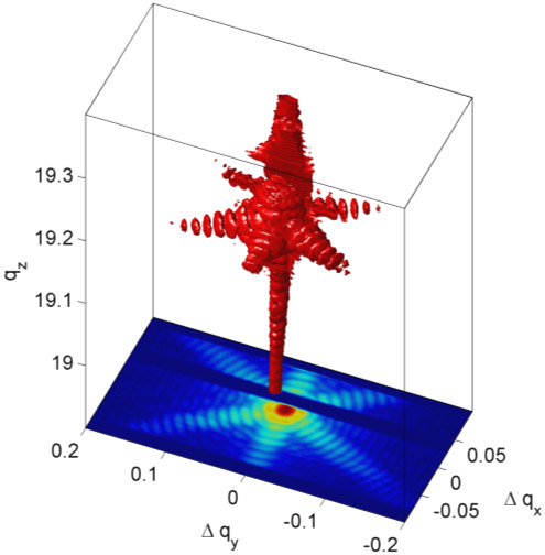
Figure 2 shows the reconstructed 3-dimensional plot of an iso-intensity surface in reciprocal space, measured at a rod inside the pattern (position 1 in Figure 1b). The qz direction in the map is parallel to the surface normal, and because the substrate’s Bragg peak is very close to the signal associated with the nanorod, parts of the data are missing due to the limited dynamic range of the detector.
 |
|
Figure 2. Three-dimensional coherent diffraction intensity distribution of a single nanorod. The red structure represents an iso-intensity surface, the map below shows a cut at constant qz through the peak from the nanorod. The region containing the substrate Bragg-maximum is missing in the data. |
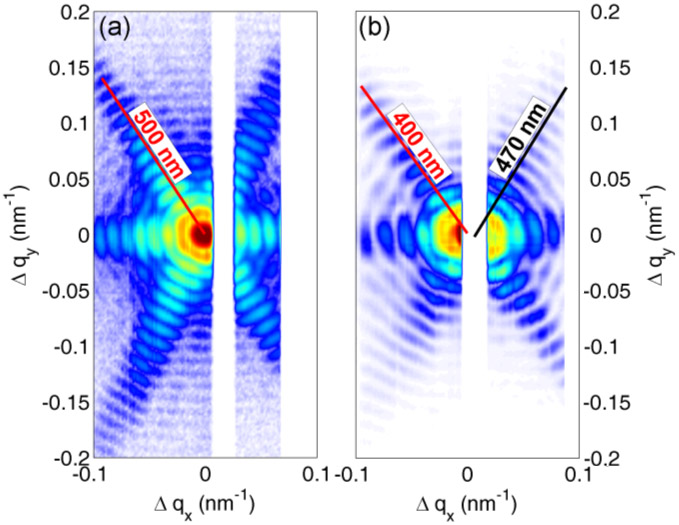
Figure 3a shows a horizontal (qx-qy) slice through the 3D diffraction pattern. Due to the coherent illumination of a single nanorod only, the diffraction pattern is the Fourier transform of the shape of the selected nanorod and shows characteristic oscillations due to the rod’s finite size and its almost perfect hexagonal symmetry in the plane parallel to the surface. In fact, the size measured by the interference fringes as indicated in Figure 3 corresponds well to the size of a single nanorod and the intensity distribution can be well described by the model of a perfect hexagon.
 |
|
Figure 3. a) Reciprocal space map taken from a rod in the centre of the array (1 in Figure 1b). b) Corresponding measurement from a rod at the border of the array. Compared to (a), the size as measured by the fringe spacing is smaller and the intensity distribution is not compatible with a perfect hexagonal distribution. |
Similar measurements were taken at nanorods at the border of the patterned array (Figure 3b), showing significant differences to the central rod. Here, the size of the rod is smaller and the shape deviates from a perfect hexagon. This supports the hypothesis that lateral material transport takes place during nanorod growth.
The data is promising for upcoming phase retrieval analysis, and should allow a detailed comparison of different nanorods. To conclude, within one sample we have been able to measure structural properties of individual nanorods with a size of few 100 nm. Our experiment gave evidence that size and shape of a nanorod are influenced by mutual material transport between neighbouring nanorods. This is in contradiction with present assumptions of nanorod growth being only vertical.
References
[1] C. Thelander et al., Materials Today 9, 28 (2006).
[2] J. Fan, P.Werner and M. Zacharias, Small 2, 700 (2006).
[3] H. Paetzelt, V. Gottschalch, J.Bauer, G.Benndorf, G.Wagner, J.Cryst. Growth 310, 5093 (2008).
[4] C. Mocuta, J. Stangl, K. Mundboth, T.H. Metzger, G. Bauer, I.A. Vartanyants, M. Schmidbauer and T. Boeck, Physical Review B 77, 245425 (2008).
[5] J. Miao, P. Charalambous, J. Kirz, and D. Sayre, Nature 400, 342 (1999).
Principal publication and authors
A. Biermanns (a), A. Davydok (a), H. Pätzelt (b,c), A. Diaz (d), V. Gottschalch (c), T.H. Metzger (d) and U. Pietsch (a), J. Synchrotron Rad. 16, 796-802 (2009).
(a) University of Siegen, Solid State Physics Group, Siegen (Germany)
(b) Leibniz Institute for Surface Modification, Ion Beam Technology Department, Leipzig (Germany)
(c) University of Leipzig, Semiconductor Chemistry Group, Leipzig (Germany)
(d) ESRF
partners


European Synchrotron Radiation Facility - 71, avenue des Martyrs, CS 40220, 38043 Grenoble Cedex 9, France.