- Home
- Users & Science
- Scientific Documentation
- ESRF Highlights
- ESRF Highlights 2000
- Microfocussing and Imaging
- X-ray Diffraction with Nanometric Spatial Resolution
X-ray Diffraction with Nanometric Spatial Resolution
The progression towards the miniaturisation and the fabrication of nano-structures requires, as an obvious consequence, the development of diagnostic techniques with high spatial resolutions. X-ray diffraction is one of the most powerful tools for the study of materials and processes, but has for long been limited to modest spatial resolution. In this study we push the spatial resolution obtainable with X-ray diffraction to the nanometric range, using X-ray waveguides (WG) as beam compressing optical elements. The WG's are multilayers of alternating layers with high and low electron density materials deposited on a flat and smooth substrate. A resonance phenomenon which strongly enhances the intensity takes place in the low density material when a collimated X-ray beam impinges upon the WG surface at an appropriate grazing angle [1].
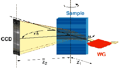
The X-ray beam exiting the WG is highly coherent in the direction perpendicular to the WG surface with spatial dimensions of the order of a few tens of nanometres. The corresponding divergence is of the order of 1 mrad. Furthermore, in the resonance condition, a strong flux density enhancement (output flux density over input flux density) takes place at the WG exit with recently achieved values as great as 100. These unique features already allowed phase contrast microradiography to be performed in a projection geometry with a record spatial resolution of about 140 nm [2]. For the microdiffraction experiment, performed at the ID13 beamline, a microelectronics structure of industrial interest was chosen, with the goal to measure, with high spatial resolution, the local strain induced on a Si substrate by sub-micrometre stripes of insulating oxide. The test samples were provided by ST-Microelectronics. The WG was placed with its surface lying in the horizontal plane, providing a line-shaped beam. The beam remains well collimated horizontally with a divergence of a few microradians, and has a vertical divergence of the order of 1 mrad. Consequently, high strain sensitivity can be achieved in the direction normal to the crystal planes if the incidence plane for Bragg diffraction is horizontal, as shown in Figure 116. In the vertical direction the desired spatial resolution could be obtained using a projection geometry. Applying suitable measurement and data analysis procedures, with the aid of phase space mapping, it was possible to measure strain depth profiles under the oxide stripes with a lateral spatial resolution of about 100 nm.
 |
Fig. 116: Set-up for X-ray diffraction with nanometre spatial resolution. The dark blue in the sample indicates the oxidised zones. The high spatial resolution is obtained in the vertical direction.
|
 |
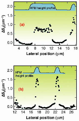
Fig. 117: Spatial variation of strain under different oxidised stripes. The experimental data indicate the position of the Si(004) reflection peak in reciprocal space as a function of the lateral position on the sample relative to the unstrained position. For comparison, the height profiles of the sample as obtained from AFM images are also included.
|
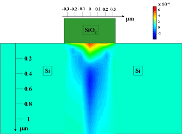
Figure 117 indicates the spatial variation of the integral strain profile under different oxidised stripes, derived from the angular positions of the diffraction peaks as measured in the experimental data. A more complex characterisation, which required the simulation of the entire set of experimental diffraction profiles, was obtained using an analytical model for the strain field description. Figure 118 shows graphically, the resulting strain field derived from the data collected under a single sub-micrometre Si oxide structure.
 |
Fig. 118: Strain field derived from the data collected under a single sub-micrometre Si oxide structure (see Figure 117b). In the colour scale, dark blue and red correspond to lattice compression and expansion respectively.
|
The potential applications of this new methodology are not limited to microelectronics materials, and interesting applications are foreseen in general in materials science for the study of the local variation of structural properties.
References
[1] W. Jark, S. Di Fonzo, S. Lagomarsino, A. Cedola, E. Di Fabrizio, A. Brahm and C. Riekel, J. Appl. Phys., 80, 4831 (1996).
[2] S. Lagomarsino, A. Cedola, P. Cloetens, S. Di Fonzo, W. Jark, G. Soullié and C. Riekel, Appl. Phys. Lett., 71, 2557 (1997).
Principal Publication and Authors
S. Di Fonzo (a), W. Jark (a), S. Lagomarsino (b), C. Giannini (c), L. De Caro (c), A. Cedola (b) and M. Muller (d), Nature 403, 638 (2000).
(a) Sincrotrone Trieste (Italy)
(b) IESS- CNR , Roma (Italy)
(c) PASTIS-CNRSM, Brindisi (Italy)
(d) ESRF


