- Home
- Users & Science
- Scientific Documentation
- ESRF Highlights
- ESRF Highlights 2000
- Surfaces and Interfaces
- "Nano-tomography" on Self-assembled Quantum Dots
"Nano-tomography" on Self-assembled Quantum Dots
The spontaneous formation of nanometer-scale islands, so-called quantum dots, during the epitaxy of semiconductor heterostructure systems with a certain lattice mismatch makes the realisation of new opto-electronic devices possible. In such quantum dots, the electrons are confined in all three directions of space, and the opto-electronic properties depend on strain, size and chemical composition. Hence, the determination of interdiffusion and strain profiles within quantum dots is of particular significance for the understanding of the growth process and for the prediction of device properties. X-ray diffraction has the potential to assess these structural parameters; however, since the very small scattering volumes contain distributions from strain and composition, a correct spatial assignment is an ambitious task.
We present a technique to identify key features of the X-ray intensity distribution in reciprocal space, allowing a transformation of scattering data to nanometer-scale real-space tomographic images of a quantum dot:
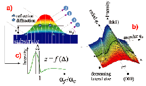
(i) If the lattice parameter varies monotonically by a few percent across the size of the dot (Figure 56a), the intensity distribution is spread out over a fairly large region of reciprocal space. The intensity at each point can be thought of as being attributed to a region of constant lattice parameter; i.e., to a slice through the quantum dot. This assignment (pseudo-resolution) decomposes the scattering from the dot into the contributions from its iso-strain areas (Figure 56b).
 |
Fig. 56: Schematic representation of the method. a) Scattering processes for a particular region of constant lateral lattice parameter at height z above the substrate. b) Simulated intensity distribution close to a surface Bragg-reflection (hk0). The colour-coding indicates the origin of the scattered intensity in (a). The dependence of lateral extent on lattice parameter is reflected by the width of the central maximum. c)
|
(ii) The height of each iso-strain area within the dot can be measured due to the presence of the surface/interface at the foot of the dots, representing a reference level. At very small angles of incidence and exit, the surface serves as a beam multiplier, allowing the X-rays to enter the detector for each of the four different scattering processes shown in Figure 56a. The coherent sum of these four amplitude terms causes the distinct shape of the intensity distribution along the exit angle (![]() f), from which the mean height above the substrate can be directly calculated with sub-nm accuracy (Figure 56c).
f), from which the mean height above the substrate can be directly calculated with sub-nm accuracy (Figure 56c).
Here, we present the results obtained from self-assembled InAs islands, grown by solid source molecular beam epitaxy on GaAs (001). The chosen growth conditions lead to rotationally symmetric quantum dots with a random lateral arrangement. Measurements in grazing incidence and exit diffraction set-up have been performed at the TROÏKA II beamline. In order to determine the 3-D structure of the dots, geometry and strain fields are extracted from 3-D intensity maps between the (220) surface Bragg-reflections of GaAs and InAs, as schematically shown in Figure 56b. At each radial position qr, a 2-D reciprocal space map is analysed in four steps [1,2]. In order to determine the chemical composition throughout the dots, the intensity distributions from a strong (400) and a weak reflection (200) along a common azimuth were compared [2].
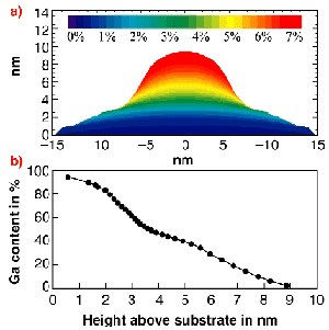
Combining all the information, we can finally draw a 3-D real-space "image" of the dot. The interdependence of shape and strain is shown in Figure 57a. The lateral lattice parameter varies from that of pure GaAs at the bottom to that of pure InAs at the top of the dot. Figure 57b shows the inter-diffusion profile as a function of the height in the dot. The Ga content of the InxGa1xAs alloy ranges from close to 100% at the dot base to 0% at the top with a remarkable large fraction of Ga in the dot centre.
 |
Fig. 57: Experimental results for the InAs/GaAs dot system: a) Magnitude of the deviation of the lateral lattice parameter from that of GaAs; b) Deduced Ga-content as a function of the height.
|
Hence the new method of "nano-tomography" allows for a quantitative determination of the composition and strain profiles of free-standing quantum dots.
References
[1] I. Kegel, T.H. Metzger, A. Lorke, J. Peisl, J. Stangl, G. Bauer, J.M. Garcia and P.M. Petroff, Phys. Rev. Lett. 85, 1694 (2000).
[2] I. Kegel, T.H. Metzger, A. Lorke, J. Peisl, J. Stangl, G. Bauer, K. Nordlund, W.V. Schoenfeld and P.M. Petroff, Phys. Rev. B 63, (2001).
Authors
T.H. Metzger (a, c), I. Kegel (a), J. Stangl (b), G. Bauer (b) and D. Smilgies (c).
(a) Ludwig-Maximilians-Universität, München (Germany)
(b) Johannes Kepler Universität, Linz (Austria)
(c) ESRF


