- Home
- Users & Science
- Scientific Documentation
- ESRF Highlights
- ESRF Highlights 2015
- Industrial research
- Innovation-led long-term project to identify critical defects in integrated circuits
Innovation-led long-term project to identify critical defects in integrated circuits
With a density of integration continuously increasing, driven by the need for better power efficiency and performance, 3D integration represents today the most promising strategy to adopt for next generation integrated circuit packaging.
Irrespective of the technology, all 3D-integrated circuits share the same challenge: to find critical defects and to verify the compliance of structural elements embedded within the bulk.
X-rays are a powerful tool for this analysis, in particular because they allow a non-destructive approach, i.e. 3D characterisation of the device, whilst the device functionality is maintained. However, nano-electronics is very demanding in terms of resolution. For this reason the use of synchrotron radiation is highly suitable to address the needs of this specific sector.
In the context of the ambitious French public-private partnership IRT “Nanoelec”, in January 2015, ST Microelectronics engaged in a three-year innovation-led long-term project (iLTP) at the ESRF, with the support of the CEA-LETI and a PhD student dedicated to the project. This collaboration focuses on advanced material characterisation, including statistical analyses, of the key interconnect and packaging technologies required in the coming generation of 3D integrated circuits. The iLTP beam time involves several of the ESRF’s nanocharacterisation beamlines, ID16A, ID01 and ID19.
In this first year of experiments, an intense campaign of nanotomography characterisation has been carried out at ID16A, with the objective to identify the potential of the nanotomographic setup and also to build up ESRF expertise and facilities (with capital contribution from the IRT Nanoelec) to effectively respond to pre-competitive and competitive applications in nano-electronics.
 |
|
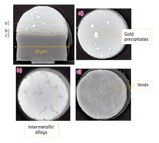
Fig. 138: Tomographic reconstruction of a 25 µm diameter copper pillar. (a)-(c) are virtual slices through the copper pillar, at various depths. |
Particular emphasis has been given to the investigation of copper pillars, some fundamental elements of the 3D-integrated circuits manufacturing technology. Copper pillars are cylinders of copper with a diameter spanning between 10 and 70 µm on which a soldering ball (Ag, Cu, Ni eutectic alloy) is deposed. One of the main results of this first year iLTP has been the tomographic acquisition of a 25 µm diameter copper pillar at the exceptional resolution of 32 nm (see Figure 138). This technique permits the main structural components of the copper pillar to be distingushed, and, in particular, the intermetallic, the control of which is one of the main concerns in the manufacturing process of these objects.
These studies result from a fruitful collaboration between A. Fraczkiewicz and P. Bleuet, CEA/LETI, F. Lorut, STMicroelectronics, and P. Cloetens and J.C. Da Silva at beamline ID16A.
Author
E. Capria.
IRT-NANOELEC, ESRF
partners


European Synchrotron Radiation Facility - 71, avenue des Martyrs, CS 40220, 38043 Grenoble Cedex 9, France.