- Home
- Users & Science
- Scientific Documentation
- ESRF Highlights
- ESRF Highlights 2014
- X-ray Imaging
- Revealing phase separation in single InGaN nanowires
Revealing phase separation in single InGaN nanowires
Semiconductor materials are evolving toward the development of more complex alloys and nanoscale heterostructures. Unexpected properties and improved functionalities can be achieved with the combination of these two approaches. For instance, the ternary alloy InxGa1-xN has an absorption edge that can be modified between 0.7 to 3.4 eV. This range covers most of the solar spectrum, making this material an excellent candidate for the development of high efficiency multijunction solar cells and light-emitting diodes. Nanometric-sized structures such as nanowires confer additional advantageous properties that can enhance the performance of the nanodevices. For instance, nanowire-shaped semiconductors absorb light in a much more efficient manner [1], and allow the possibility to build core−shell structures that further improve the performance of solar cells [2], and light-emitting devices [3].
Characterisation of these complex nanoscale structures requires the combination of several techniques, preferably with a high spatial resolution to avoid the averaging that could hide local details. In this work, we have used the hard X-ray nanoprobe at beamline ID22NI (now at ID16B) to characterise self-assembled single InxGa1-xN nanowires using a multi-technique approach and nanometric resolution.
 |
|
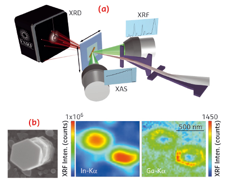
Fig. 57: (a) Multi-technique setup at the nanoimaging station ID22NI (now at beamline ID16B). (b) SEM image (left), In (centre) and Ga (right) Kα XRF maps of representative single as-grown nanowires on the Si substrate taken from the top. |
Figure 57a shows a schematic view of the setup at the X-ray nanoprobe, which integrates X-ray fluorescence (XRF), X-ray diffraction (XRD) and X-ray absorption spectroscopy techniques. This multi-technique approach allows the simultaneous study of the composition, long- and short-range order of the samples, with a very high lateral spatial resolution. As-grown and dispersed nanowires placed onto thin membranes were scanned with both, pink (ΔE/E ~ 10-2, flux of ~ 5 × 10¹² ph/s, 55 × 55 nm2 spot size) and monochromatic (ΔE/E ~ 10-4, flux of ~ 5 × 10¹⁰ ph/s, 105 × 110 nm2 spot size) beams. XRF maps of the nanowires show an axial and radial elemental heterogeneity with Ga accumulation in the bottom and in the outer region of the nanowire, examples are displayed in Figure 57b.
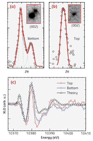
Nano-XRD and nano-XRF maps were performed simultaneously on single dispersed nanowires, using a 28 keV monochromatic beam. Figure 58 shows the XRD spectra of the InGaN (002) reflection acquired at the bottom (a) and top (b) of a single nanowire. A closer inspection of the (002) reflection shows at least three Gaussian contributions to this XRD peak at the bottom, and single Gaussian-like XRD peak at the top. These different contributions to the (002) diffraction peak are observed even in the original CCD images, shown in the insets of Figure 58a and b. Finally, X-ray linear dichroism (XLD) spectra around the Ga K-edge measured at the top and bottom of a single nanowire, and the calculated spectrum for wurtzite GaN are shown in Figure 58c. Both XLD spectra of the nanowire exhibit the strong anisotropy of the X-ray absorption, typical for the wurtzite GaN matrix. This confirms that despite the elemental modulation, the tetrahedral order around the Ga absorbing atoms remains along the nanowires.
 |
|
Fig. 58: (a) InGaN (002) XRD reflection (open circles) acquired at the bottom (a) and top (b) of a single nanowire along with the best multi-Gaussian fits (solid line). Different Gaussian contributions are plotted with dotted lines. The insets show the corresponding CCD images. (c) XLD spectra around the Ga K-edge measured at the top (squares) and bottom (circles) of a single nanowire, and the calculated spectrum (triangles) for wurtzite GaN. |
In conclusion, a large phase separation at the bottom, and a single phase at the top of the nanowires were revealed. We anticipate that this methodology will contribute to a greater understanding of the underlying growth concepts, not only of nanowires, but also of many nanostructures in materials science.
Principal publication and authors
J. Segura-Ruiz (a, b), G. Martinez-Criado (a), C. Denker (c), J. Malindretos (c), A. Rizzi (c), Nano Lett. 14, 1300−1305 (2014).
(a) ESRF
(b) Present address: Institut Laue-Langevin, Grenoble (France)
(c) IV. Physikalisches Institut, Georg-August-Universität Göttingen, (Germany)
References
[1] J. Wallentin, N. Anttu, D. Asoli, M. Huffman, I. Åberg, M.H. Magnusson, G. Siefer, P. Fuss-Kailuweit, F. Dimroth, B. Witzigmann, H.Q. Xu, L. Samuelson, K. Deppert and M.T. Borgström, Science 339, 1057−1060 (2013).
[2] M.D. Kelzenberg, S.W. Boettcher, J.A. Petykiewicz, D.B. Turner-Evans, M.C. Putnam, E.L. Warren, J.M. Spurgeon, R.M. Briggs, N.S. Lewis and H.A. Atwater, Nat. Mater. 9, 239−244 (2010).
[3] G. Martínez-Criado, A. Homs, B. Alén, J.A. Sans, J. Segura-Ruiz, A. Molina-Sánchez, J. Susini, J. Yoo and G.-C. Yi, Nano Lett. 12, 5829−5834 (2012).


